Having reference designators and silkscreen outlines readable on a PCB is crucial for assembly, testing, and troubleshooting. However, these features are often drawn on different subclasses. To ensure reference designators are included on the correct silkscreen layers for manufacturing, designers can automatically generate a silkscreen for the PCB. OrCAD X PCB Designer includes Auto Silkscreen to easily generate silkscreen and fill a common layer containing all silkscreen elements for each side of the board.
This quick how-to will provide step-by-step instructions on how to automatically generate a silkscreen on a single layer for each side of the board with Auto Silkscreen in OrCAD X PCB Designer.
To follow along, download the provided files above the table of contents.
How-To Video
 Open in New Window
Activating Auto Silkscreen
Step 1: Open the provided design in OrCAD X PCB Designer.
Step 2: Select Manufacture > Silkscreen from the menu to open the Auto Silkscreen window.
Automatically Generate Silkscreen: Configuring Settings
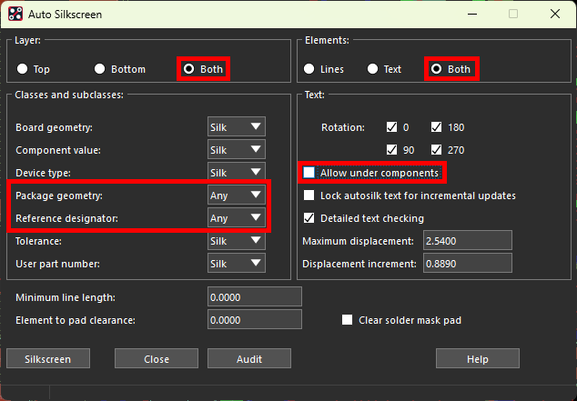
Step 3: The Auto Silkscreen window opens. Here you can configure where the silkscreen is displayed and for which elements, the classes and subclasses to draw the silkscreen information from, and how to orient the text.
Select Both under Layer and Both under elements to plot lines and text on both layers.
Step 4: Under Classes and Subclasses, select Any from the Package Geometry and Reference Designator dropdown. This will draw package geometry and reference designators from the silkscreen or assembly subclasses.
Step 5: Uncheck the option for Allow Under Components to prevent the silkscreen from being hidden by soldered components in the final board.
Note: Other configurable settings in this window include text rotation, text checking, and displacement.
Automatically Generate Silkscreen: Auditing
Step 6: An audit file can be generated for a silkscreen before the silkscreen itself is created. This audit file contains any errors and warnings that will be generated with the silkscreen in its current configuration. Select Audit.
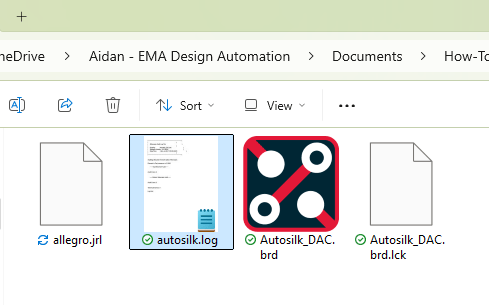
Step 7: The Auto Silkscreen window closes automatically. Open File Explorer and browse to the working directory. A new autosilk.log file is shown.
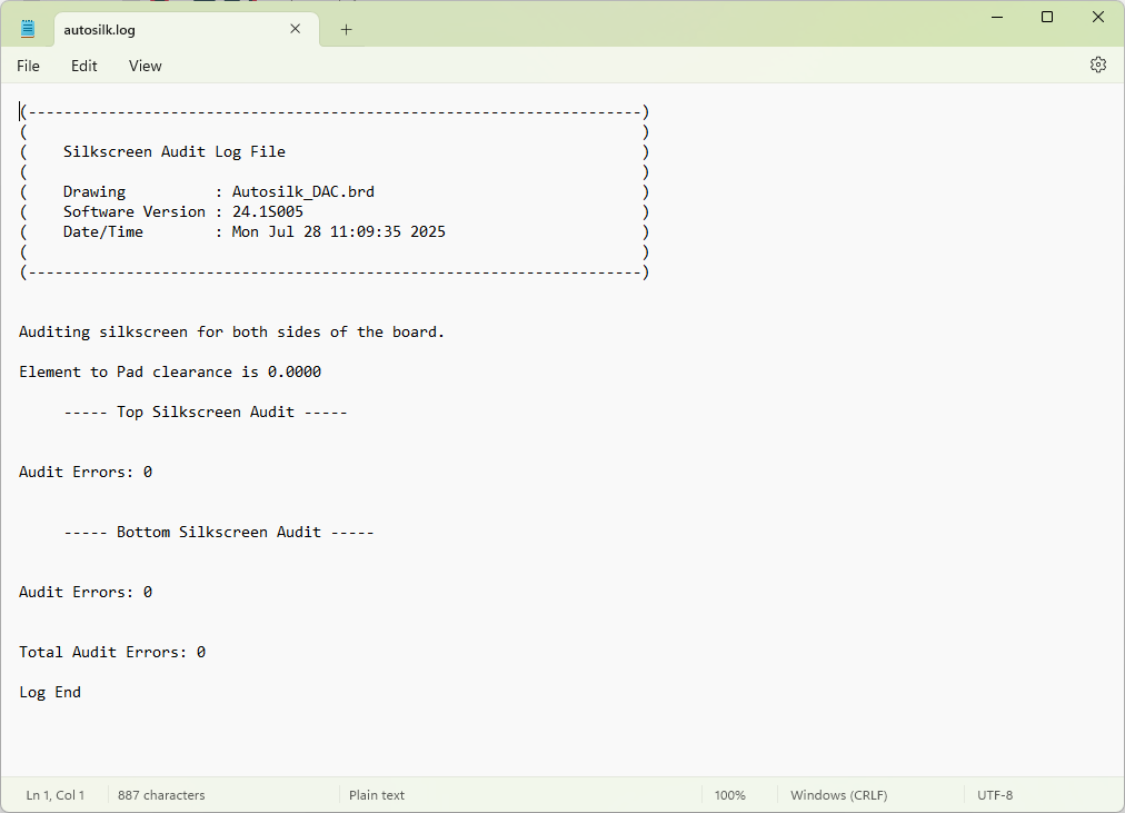
Step 8: Open the file in a text editor such as Notepad. The file shows the name of the board the silkscreen is from, the date and time, and the number of errors on each side. No errors were generated for this board.
Step 9: Close the text editor.
Automatically Generate Silkscreen
Step 10: Back in OrCAD X PCB Designer, select Manufacture > Silkscreen again to reopen the Auto Silkscreen window.
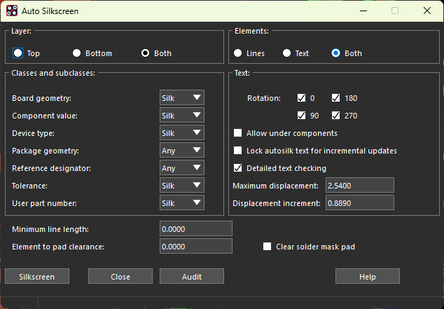
Step 11: If any settings reset to the defaults, reconfigure them as shown above.
Step 12: Click Silkscreen to generate the silkscreen. The Auto Silkscreen window closes automatically.
Viewing the Silkscreen
Step 13: The autosilk layers are not shown by default. To view them, select the Color icon from the toolbar.
Step 14: The Color dialog window opens. Select Manufacturing from the category list on the left.
Step 15: Check the option for Autosilk_Bottom. The newly-generated bottom silkscreen is shown in the PCB canvas. Look for the capacitors under the larger QFP IC.
Note: If your system has multiple monitors, put the Color Dialog window in another monitor. Otherwise, minimize the window.
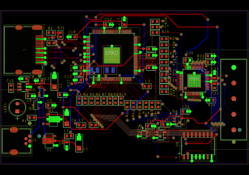
Step 16: Uncheck the option for Autosilk_Bottom and check Autosilk_Top. Silkscreen generated on the top of the board is shown.
Step 17: Click OK to leave the silkscreen enabled and close the Color Dialog window.
Wrap Up & Next Steps
Automatically generate silkscreen layers to ensure the correct silkscreen is printed to your board during manufacturing and clear communication of reference designators for assembly and testing with OrCAD X PCB Designer. Test this feature and more with a free trial of OrCAD. Get more how-tos for OrCAD at EMA Academy.

