Planes and copper pours are essential in PCB design to ensure robust power connections and low noise in a design. The dynamic healing feature in OrCAD X makes creating shapes quick and easy at any point in the design process including the ability to change the fill radius of dynamic copper shapes to meet manufacturing and electrical requirements.
This quick how-to will provide step-by-step instructions on how to change the fill radius of dynamic copper shapes in OrCAD X PCB Designer.
To follow along, download the provided files above the table of contents.
How-To Video
 Open in New Window
Change the Fill Radius of Dynamic Copper Shapes
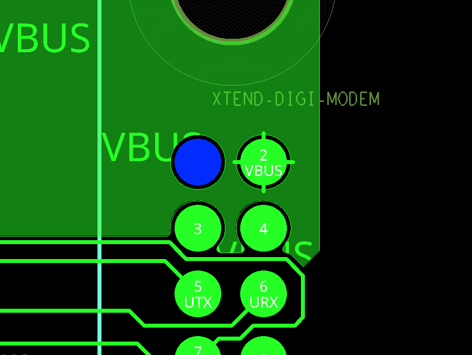
Step 1: Open the provided design in OrCAD X PCB Designer. Navigate to the top pins of JP1 on the PCB. In this scenario, we want to change the radius of the copper pour.
Step 2: The global design fill radius can be configured from the Design Parameter Editor window. Select Setup > Design Parameters from the menu.
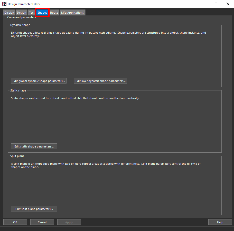
Step 3: The Design Parameter Editor window opens. Select the Shapes tab.
Step 4: Select Edit Global Dynamic Shape Parameters.
Note: Shape parameters can be adjusted by layer under Edit Layer Dynamic Shape Parameters.
Step 5: The Global Dynamic Shape Parameters window opens. Select the Void Controls tab.
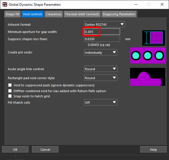
Step 6: The Void Controls panel opens, showing spacing options for the selected artwork format. Shape suppression, gap width, and pin void options can be set from this panel.
Enter 0.381 for the Minimum Aperture for Gap Width to increase the radius of the void corners.
Step 7: Click OK in the Global Dynamic Shape Parameters and Design Parameter Editor windows.
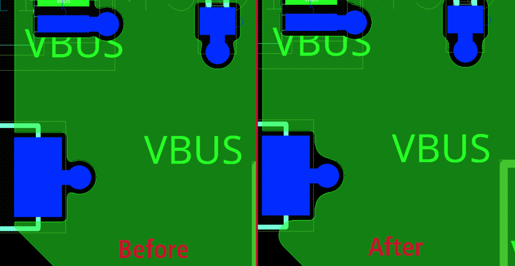
Step 8: View the PCB canvas. The copper cutouts for the through-hole pins on the right side of the VBUS plane have been widened. The widening has created shape islands, which result in DRC errors. This will be corrected in the following steps.
Deleting Shape Islands
Step 9: Select Shape > Delete Unconnected Copper from the menu.
Step 10: The shape islands are highlighted and the Options panel is populated with layer options. Select Delete All On Layer to remove all shape islands on the active layer.
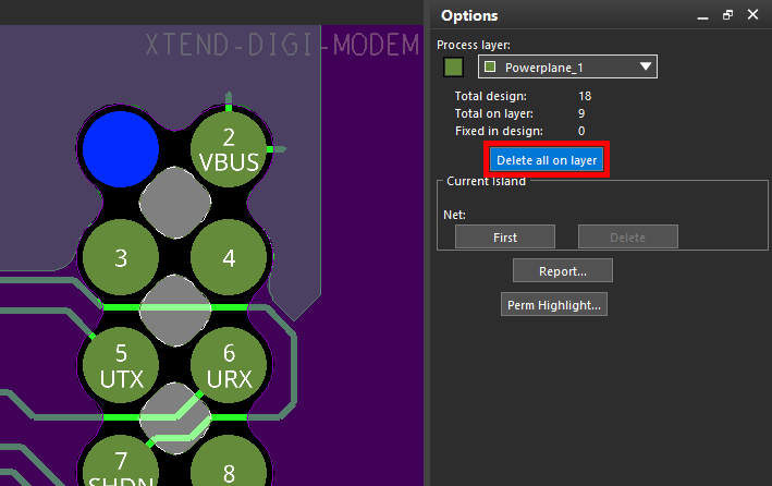
Step 11: Select layers Powerplane_1 and Bottom and click Delete All On Layer to clear shape islands from the 3.3V and ground planes.
Step 12: Right-click and select Done.
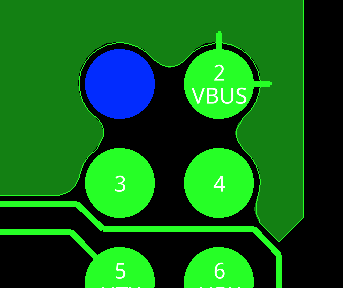
Step 13: In the Visibility panel, uncheck the option under All for Powerplane_1 and Bottom to turn visibility off for those layers. The shape islands have been removed from the area around JP1.
Wrap Up & Next Steps
Quickly and easily change the fill radius of dynamic copper shapes at a global, layer, or net level in OrCAD X PCB Designer. Test out this feature and more with a free trial of OrCAD X. Get more how-tos for OrCAD X at EMA Academy.

