With today’s designs becoming more compact and layer counts increasing, routing intricacies increase requiring complex rules and vias to meet performance and functionality requirements. For example, long vias can create antennas in high-speed nets, potentially affecting signal integrity by creating impedance discontinuities. Blind and buried vias can be used to limit via space to two or more layers and reduce antenna length. With OrCAD X PCB Designer Professional, easily create blind and buried vias to ensure your design remains manufacturable and impedance discontinuities are reduced.
This quick how-to will provide step-by-step instructions on how to create blind and buried vias in OrCAD X PCB Designer.
To follow along, download the provided files above the table of contents.
How-To Video
 Open in New Window
Create Blind and Buried Vias
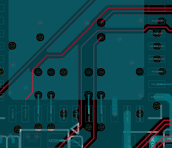
Step 1: Open the provided design in OrCAD X PCB Designer Professional.
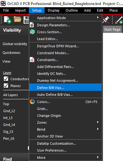
Step 2: Select Setup > Define B/B Vias to open the Blind/Buried Vias window.
Step 3: The Blind/Buried Vias window opens. Here you can define all blind/buried vias to be used in the design, their padstack base, and the layers they span. For this example, we will create a via from the top layer to INT_L3.
Select Add BBVia.
Step 4: A new blind/buried via is added to the list. Enter VIA_BB_13 for the name.
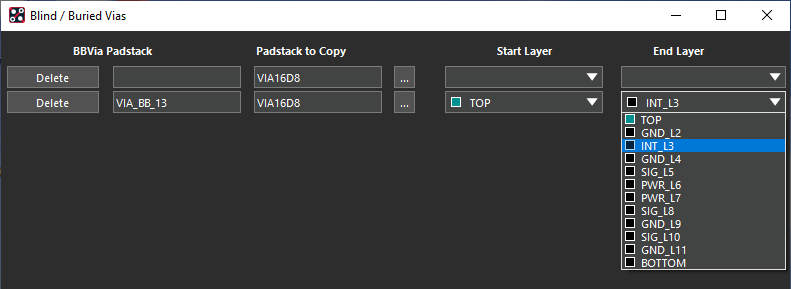
Step 5: For the new via, select TOP from the Start Layer dropdown and INT_L3 from the End Layer dropdown.
Step 6: Click OK to save the new via and close the window.
Blind and Buried Vias: Design Rules
Step 7: Before the via can be placed in the design, it needs to be assigned to the default constraint set so it is shown in the via placement lists. Select Setup > Constraints from the menu.
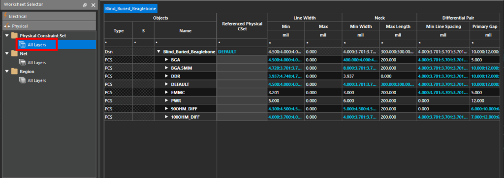
Step 8: The Constraint Manager opens. Select the Physical domain from the Worksheet Selector and the Physical Constraint Set > All Layers worksheet.
Step 9: The Physical Constraint Set > All Layers worksheet lists all physical constraint rules for this design. Scroll to the column with Vias as a header and double-click the corresponding cell for Default to edit the default via settings.
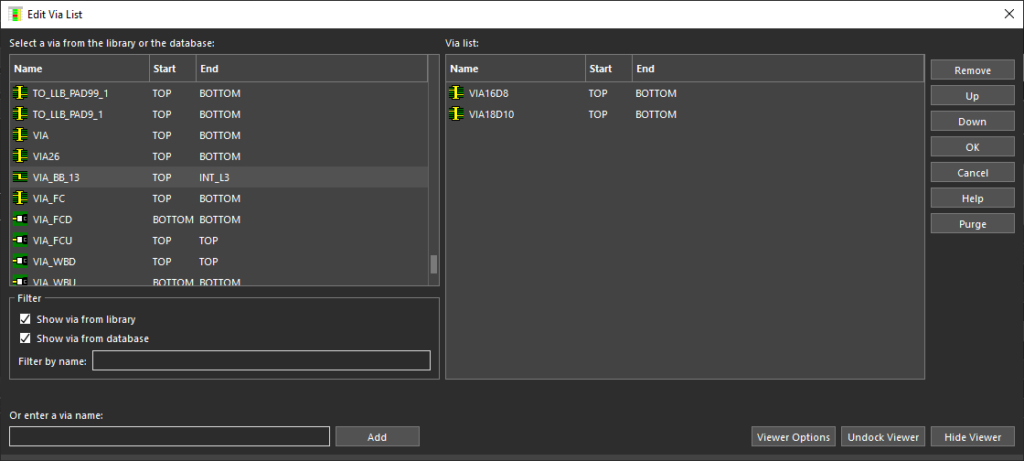
Step 10: The Edit Via List window opens. Here you can define which vias to use in the design and which can be used with each layer or feature. In the via selection table on the left, scroll down to VIA_BB_13.
Step 11: Double-click the via to add it to the Via List on the right. The via can now be incorporated into the design.
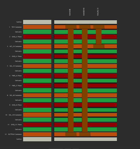
Note: The pictorial in the bottom-right of the screen indicates the via structure for enabled vias. In this case, the first two vias span the whole board while the newly-added via stops at L3.
Step 12: Click OK to save the changes and close the window.
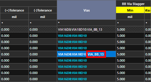
Step 13: Look at the Vias cell for Default in the Constraint Manager again. VIA_BB_13 is now added as an acceptable via.
Step 14: Close the Constraint Manager.
Routing with Blind and Buried Vias
Step 15: There are two unconnected nets on this board that can be routed with the new via. Select Route > Connect from the menu.
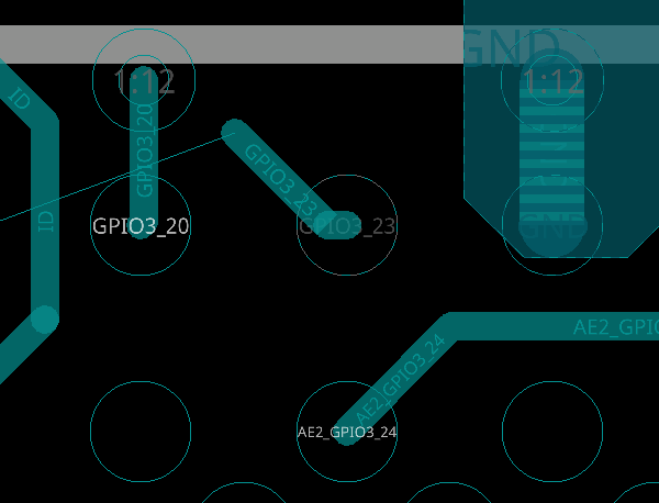
Step 16: Select pin GPIO3_23 on U4. A trace is attached to your cursor.
Step 17: In the Options panel, select Int_L3 from the alternate layer list. VIA_BB_13 is automatically selected as the active via.
Step 18: In the Visibility panel, check the box under All for Int_L3 to enable visibility for Layer 3.
Step 19: Double-click to create a via and start routing on Layer 3. The blind/buried via is created.
Note: The layer span numbers in the via show 1:3.
Step 20: Click to route the trace to the GPIO3_23 pad on U37, as guided by the ratsnest line.
Step 21: Double-click to create another blind/buried via under the pad. The net is connected.
Routing with Blind and Buried Vias: Working Layer Mode
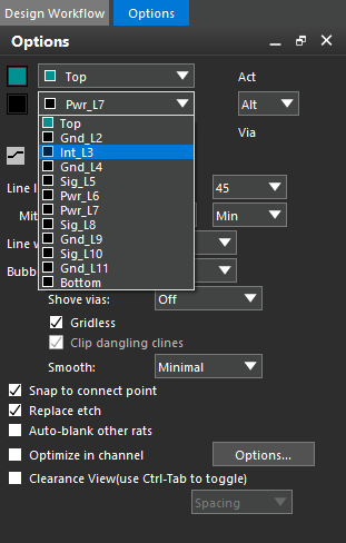
Step 22: Blind and buried vias can also be added in the Working Layer (WL) mode. Select WL from the mode dropdown in the Options panel.
Step 23: Select pin GPIO3_18 on U4 to start routing. Double-click to open the Add Via window.
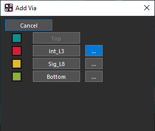
Step 24: In the Add Via window, select the ellipsis for Int_L3.
Step 25: An alternate via list is shown. Select Via_BB_13.
Step 26: The via is placed. Continue routing on Layer 3, following the ratsnest line to the pad on U37.
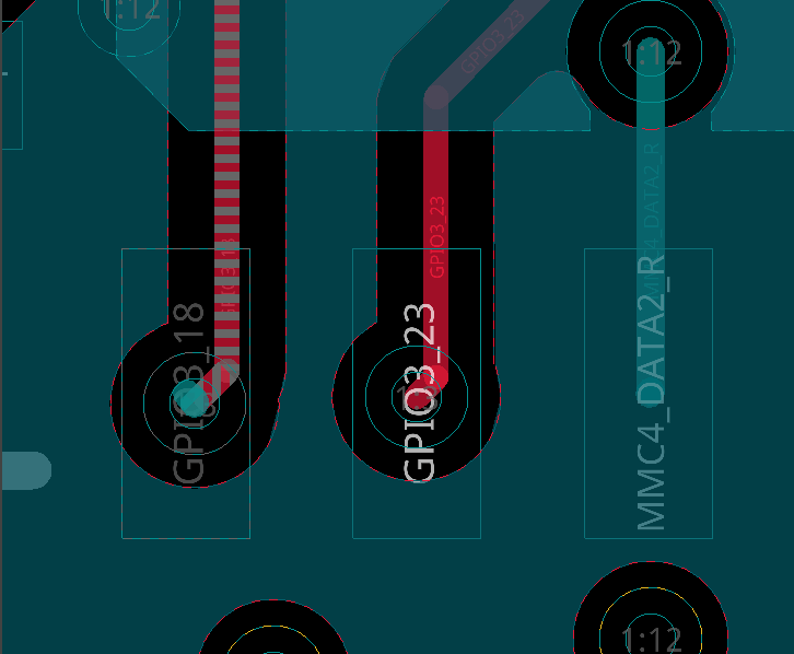
Step 27: Double-click to open the Add Via window. Select the ellipsis for Top and choose Via_BB_13 from the alternate via list. Click to finish the trace as a via-in-pad.
Step 28: Right-click and select Done. The board is routed with blind and buried vias.
Wrap Up & Next Steps
Quickly and easily create blind and buried vias to preserve signal integrity and space in OrCAD X PCB Designer. Test this feature and more with a free trial of OrCAD. Get more how-tos for OrCAD at EMA Academy.

