
Defining Electrical Rules for Differential Pairs
Step 1: Open the provided design in OrCAD X Presto.
Step 2: If the Constraints panel is not visible, select View > Panels > Constraints from the menu.
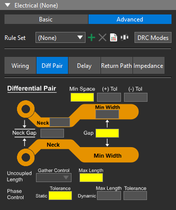
Step 3: The Constraints panel opens on the right side of the PCB canvas. Select Advanced under Electrical to define advanced electrical rules including:
-
Wiring
-
Differential Pairs
-
Propagation Delay
-
Return Path
-
Impedance
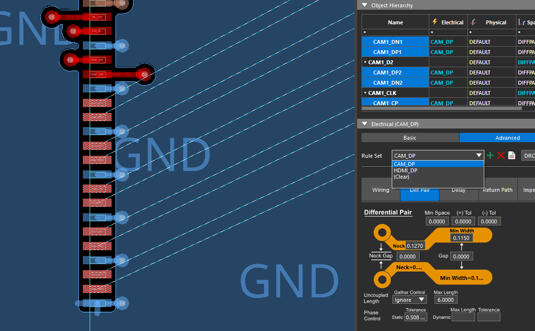
Step 4: Select Differential Pair to define a differential pair rule set.
Creating a Differential Pair CSet
Step 5: Select the plus sign for Create Electrical CSet to create a new constraint set.
Step 6: The Create Electrical CSet window opens. Enter CAM_DP for the name.
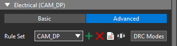
Step 7: Click OK. The constraint set is automatically selected from the Rule Set dropdown.
Step 8: Select Ignore from the Gather Control dropdown towards the bottom of the subpanel. This option determines whether to include or ignore decoupling for pin connections in the uncoupled length.
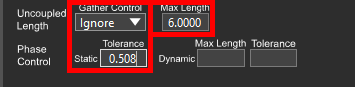
Step 9: Set the Maximum Uncoupled Length to 6. This will set the maximum uncoupled length or the maximum length at which the routed differential pair traces can be spaced farther than their assigned primary gap, to 6mm.
Step 10: Set the Static Phase Tolerance to 0.508. This defines the maximum distance for the differential pair to be out of phase to 0.508mm.
Assigning Electrical Rules for Differential Pairs
Step 11: The differential pair constraint set must be assigned to the appropriate nets before it can be checked. In the Selection Filter subpanel, disable All Objects and enable Nets to allow the selection of nets.
Step 12: Click and drag to select all CAM1 pads on connector J11 on the left side of the board. Hold CTRL and click the GND plane to deselect it. The Constraints panel is populated with common constraints for these nets.
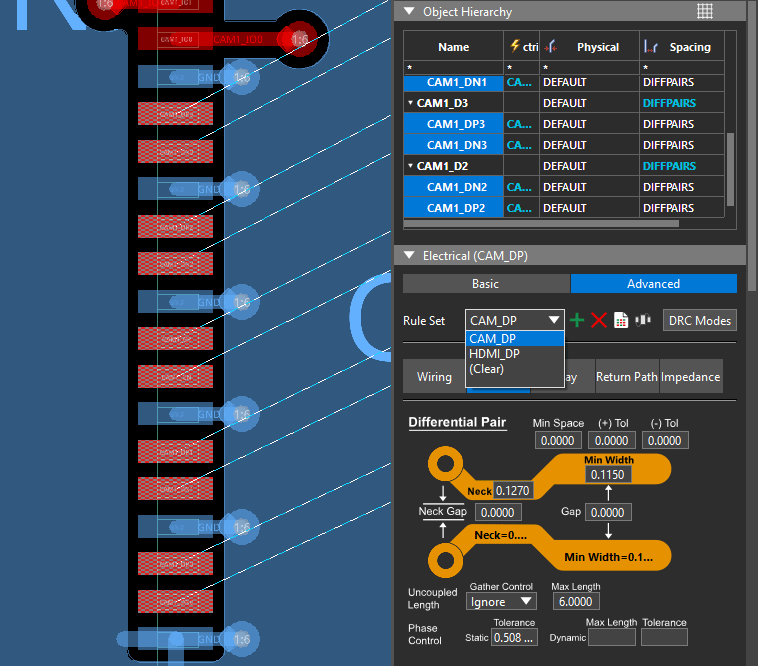
Step 13: Select CAM_DP from the Rule Set dropdown. The constraint set is assigned to all CAM1 nets.
Step 14: Click anywhere to deselect the nets.
Defining Physical Rules for Differential Pairs
Step 15: Physical rules such as minimum line width and primary gap can be assigned for differential pairs as well, and constraints can also be defined and assigned in the Constraint Manager. Select Electrical Analysis > Constraint Manager from the menu to activate the Constraint Manager.
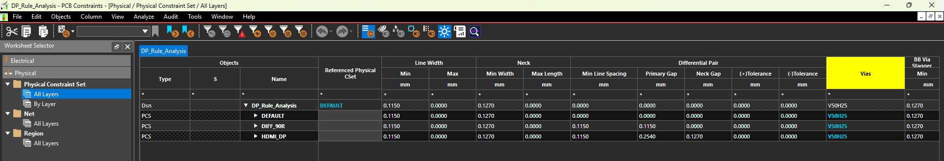
Step 16: The Constraint Manager window opens, showing a directory of constraint domains and worksheets. Select the Physical domain.
Step 17: Select the Physical Constraint Set > All Layers worksheet.
Step 18: Right-click the Default constraint set and select Create > Physical CSet.
Step 19: Enter CAM_DP for the name and click OK to create the constraint set.
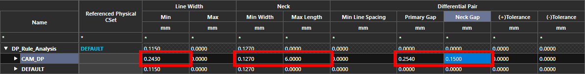
Step 20: Assign the following constraint values:
-
Line Width: 0.243
-
Primary Gap: 0.254
-
Neck Length: 6
-
Neck Width: 0.127
-
Neck Gap: 0.15
Assigning Physical Rules for Differential Pairs
Step 21: Physical constraint sets must also be assigned to their relevant nets to be checked. Select the Net > All Layers worksheet in the Physical domain.
Step 22: A list of nets and their assigned physical constraint set opens. Click and drag to select the cells under Referenced Physical CSet for all CAM1 differential pair objects.
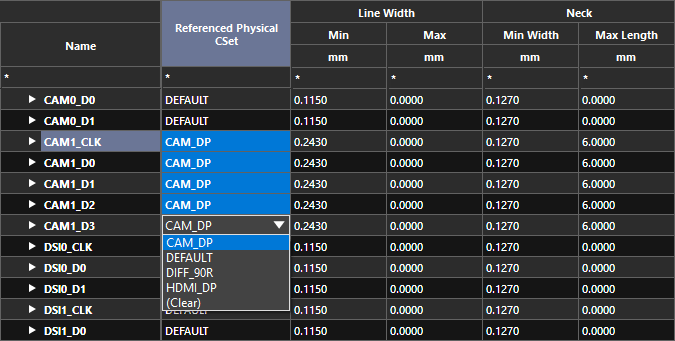
Step 23: Select CAM_DP from the resulting dropdown. The CAM_DP CSet is assigned to all selected differential pairs. The physical constraint sets are assigned.
Activating Analysis for Differential Pair Rules
Step 24: Before the differential pair checks are run on the board, they must be enabled. Select Analyze > Analysis Mode from the Constraint Manager menu.
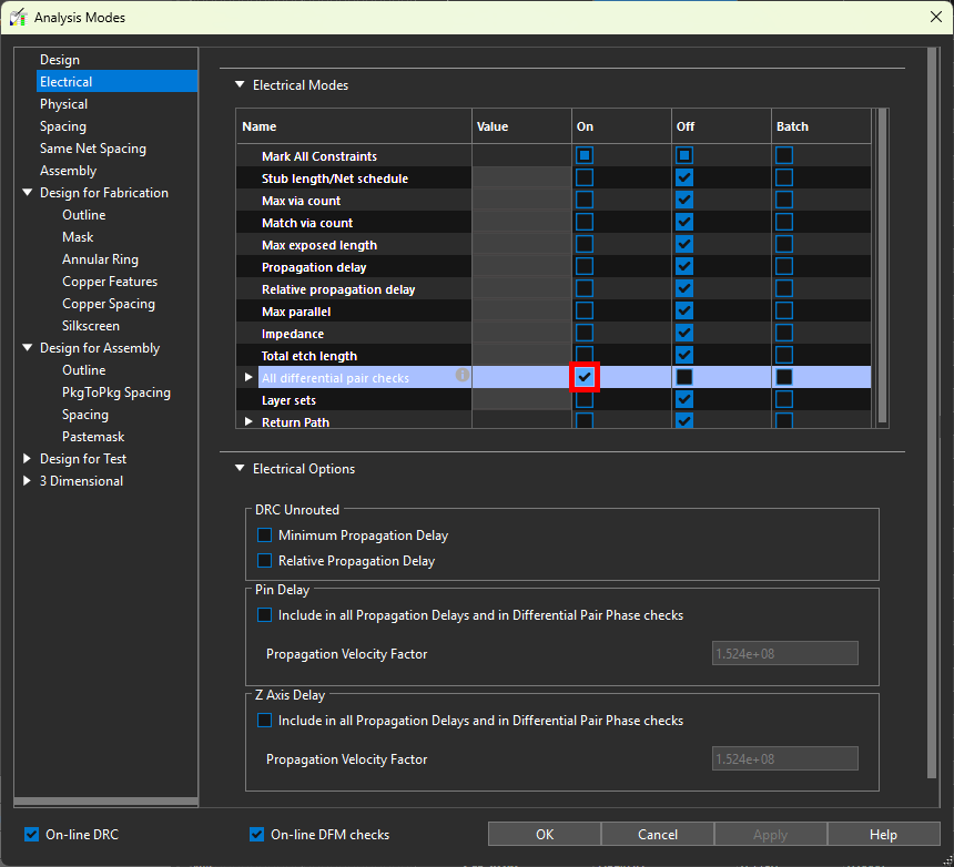
Step 25: The Analysis Modes window opens. Here you can enable all design rule checks available in OrCAD X PCB Designer. Select Electrical from the list on the left.
Step 26: Select the checkbox under On for All Differential Pair Checks. All differential pair checks are enabled.
Step 27: Click OK to save the settings and close the window.
Step 28: Minimize the Constraint Manager.
Routing Differential Pairs in OrCAD X
Step 29: To route the nets, choose the Add Connect mode from the toolbar.
Step 30: In the Add Connect widget, select Assisted from Route Mode.
Step 31: Enable Pins in the Selection Filter subpanel to allow pins to be selected.
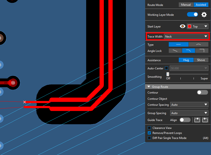
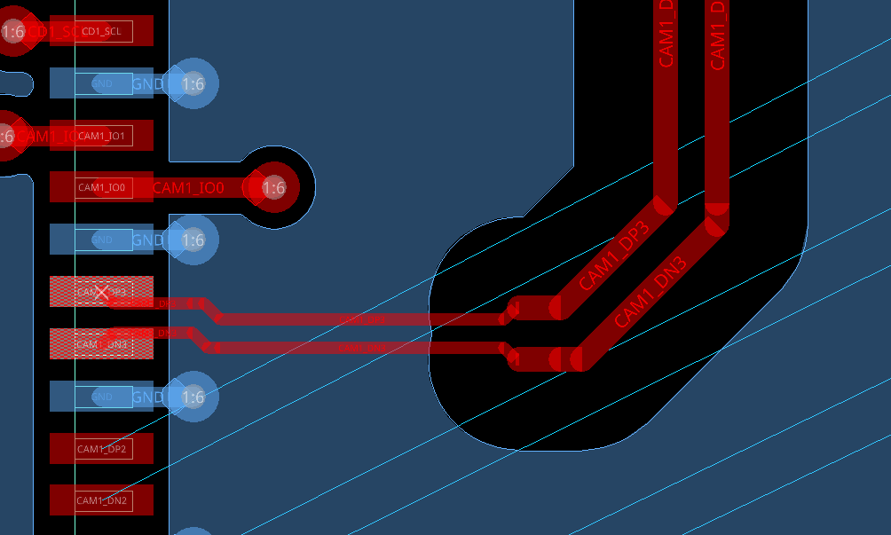
Step 32: Click one of the pins to start routing. Both traces of the differential pair are attached to your cursor. The constraints have been automatically assigned for line width and gap.
Step 33: Click to route the traces. Select Neck from the Trace Width dropdown to neck down. The constraints for the neck width and neck gap have been automatically assigned.
Step 34: Complete the differential pair routing by connecting them to the corresponding pads as indicated by the ratsnest lines. When finished, choose the Select mode from the toolbar.
Step 35: Reopen the Constraint Manager. Select the Electrical domain and the Net > Routing > Differential Pair worksheet.
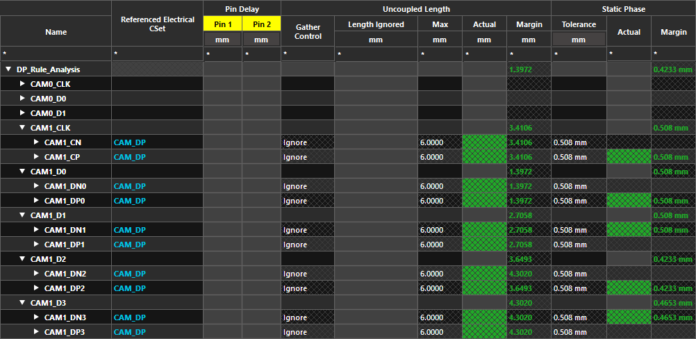
Step 36: Expand the CAM1 differential pair objects and nets and view the actual uncoupled length. All values are green, indicating they are passing.
Defining Electrical Rules for Differential Pairs
Step 1: Open the provided design in OrCAD X PCB Designer.
Step 2: If the Constraints panel is not visible, select Display > Windows > Constraints from the menu.
Step 3: The Constraints panel opens on the right side of the PCB canvas. Select Advanced under Electrical to define advanced electrical rules including:
-
Wiring
-
Differential Pair
-
Propagation Delay
-
Return Path
-
Impedance
Step 4: Select Differential Pair to define a differential pair rule set.
Creating a Differential Pair CSet
Step 5: Select the plus sign for Create Electrical CSet to create a new constraint set.
Step 6: The Create Electrical CSet window opens. Enter CAM_DP for the name.
Step 7: Click OK. The constraint set is automatically selected from the Rule Set dropdown.
Step 8: Select Ignore from the Gather Control dropdown towards the bottom of the subpanel. This option determines whether to include or ignore decoupling for pin connections in the uncoupled length.
Step 9: Set the Maximum Uncoupled Length to 6. This will set the maximum uncoupled length or the maximum length at which the routed differential pair traces can be spaced farther than their assigned primary gap, to 6mm.
Step 10: Set the Static Phase Tolerance to 0.508. This defines the maximum distance for the differential pair to be out of phase to 0.508mm.
Assigning Electrical Rules for Differential Pairs
Step 11: The differential pair constraint set must be assigned to the appropriate nets before it can be checked. In the Find panel, select All Off and check Nets to allow the selection of nets.
Step 12: Click and drag to select all CAM1 pads on connector J11 on the left side of the board. Hold CTRL and click the GND plane to deselect it. The Constraints panel is populated with common constraints for these nets.
Step 13: Select CAM_DP from the Rule Set dropdown. The constraint set is assigned to all CAM1 nets.
Step 14: Click anywhere to deselect the nets.
Defining Physical Rules for Differential Pairs
Step 15: Physical rules such as minimum and primary gap can be assigned for differential pairs as well, and constraints can also be defined and assigned in the Constraint Manager. Select Setup > Constraints from the menu to activate the Constraint Manager.
Step 16: The Constraint Manager window opens, showing a directory of constraint domains and worksheets. Select the Physical domain.
Step 17: Select the Physical Constraint Set > All Layers worksheet.
Step 18: Right-click the Default constraint set and select Create > Physical CSet.
Step 19: Enter CAM_DP for the name and click OK to create the constraint set.
Step 20: Assign the following constraint values:
-
Line Width: 0.243
-
Neck Width: 0.127
-
Neck Length: 6
-
Primary Gap: 0.254
-
Neck Gap: 0.15
Assigning Physical Rules for Differential Pairs
Step 21: Physical constraint sets must also be assigned to their relevant nets to be checked. Select the Net > All Layers worksheet in the Physical domain.
Step 22: A list of nets and their assigned physical constraint set opens. Click and drag to select the cells under Referenced Physical CSet for all CAM1 differential pair objects.
Step 23: Select CAM_DP from the resulting dropdown. The CAM_DP CSet is assigned to all selected differential pairs.
Activating Analysis for Differential Pair Rules
Step 24: Before the differential pair checks are run on the board, they must be enabled. Select Analyze > Analysis Mode from the Constraint Manager menu.
Step 25: The Analysis Modes window opens. Here you can enable all design rule checks available in OrCAD X PCB Designer. Select Electrical from the list on the left.
Step 26: Select the checkbox under On for All Differential Pair Checks. All differential pair checks are enabled.
Step 27: Click OK to save the settings and close the window.
Routing Differential Pairs in OrCAD
Step 28: Minimize the Constraint Manager.
Step 29: Scroll up to zoom into the CAM1 nets on the PCB canvas.
Step 30: Select Route > Connect from the menu.
Step 31: Click one of the unrouted pads to start routing a differential pair using the ratsnest lines as a guide. Both nets in the pair are attached to your cursor and routed together. A heads-up display is shown to ensure adherence to the static phase tolerance constraint.
Step 32: Right-click and check Neck Mode to neck down. The constraints for the neck width and neck gap have been automatically assigned. Click the end pad to finish.
Step 33: Complete the differential pair routing by connecting the traces to the corresponding pads as indicated by the ratsnest lines. When finished, right-click and select Done.
Step 34: Reopen the Constraint Manager.
Step 35: Select the Electrical domain and the Net > Routing > Differential Pair worksheet. Expand the CAM1 differential pair objects and nets and view the actual uncoupled length. All values are green, indicating they are passing.

