When completing a PCB design, it is important to obtain a summary of the design to determine your PCB design statistics and verify accuracy. PCB design statistics can include:
- Layers and design thickness
- Number of padstacks
- Minimum drill size
- Number of holes in the design (plated and unplated)
- Drilling requirements for holes and vias
- Completed and missing connections
- Number of placed and unplaced components
- Trace summary
This information helps to verify the design is completed and communicate critical design information to stakeholders and manufacturers. OrCAD X allows you to create a summary report containing your PCB design statistics for efficient review of critical design information.
This quick how-to will provide step-by-step instructions on how to determine your PCB design statistics by creating a summary drawing report in OrCAD X.
To follow along, download the provided files above the table of contents.
How-To Video
 Open in New Window
Determining Your PCB Design Statistics
Step 1: Open the desired design in OrCAD X PCB Designer.
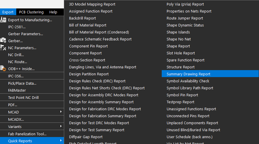
Step 2: Select Export > Quick Reports > Summary Drawing Report from the menu.
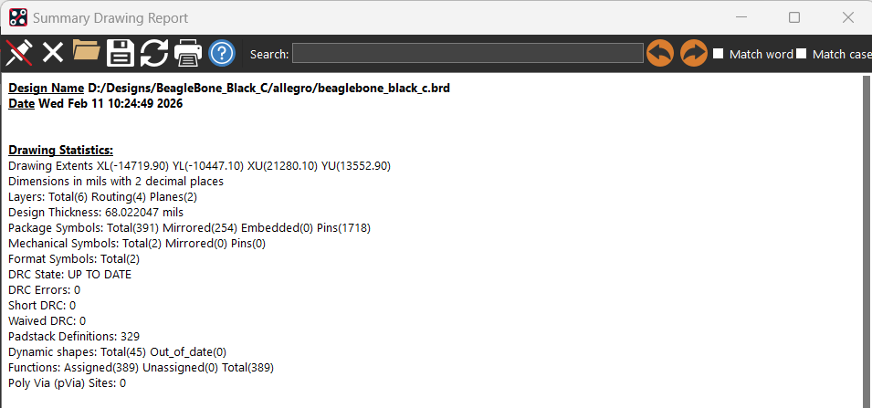
Step 3: View the Drawing Statistics. Information reported here includes:
- Total Layers
- Design Thickness
- Total Package Symbols and Mechanical Symbols
- Design Rule Check Information
Step 4: View the Drilling Statistics. Information reported here includes:
- Minimum drill size
- Number of drills, standard and non-standard
- Number of holes, plated and non-plated
- Number of vias
Step 5: View the Connection Statistics. Information reported here includes:
- Number of connects
- Completed connections
- Missing connections
- Dangling connections
- Trace length
Step 6: View the Layout Statistics. Information reported here includes:
- Components
- Component class breakdown
- Route keepin
- Pins
- Layout Area
- Pin Density
Step 7: View the Trace Layer Statistics. Information reported here includes:
- Board layers
- Number of clines per layer
- Number of shapes per layer
- Number of component pins per layer
Step 8: View the Trace Widths By Layer. Information reported here includes:
- Board layers
- Trace width per layer
Step 9: Verify the completeness of the design and accuracy. Additionally, this information can be used for reporting, design reviews, manufacturing and software quoting, and more. Save or Print the Summary Design Report as required then close the window.
Wrap Up & Next Steps
Quickly obtain a summary of the design to determine your PCB design statistics and efficiently review critical design information with the Summary Drawing Report in OrCAD X. Don’t have OrCAD X? Get a free trial here and get more step-by-step instructions at EMA Academy.

