Electromagnetic Interference (EMI) and noise can have a detrimental effect on design performance. Using vias to shield the entire board or aspects of the design can prevent external influences as well as noisy circuits on the PCB from effecting functionality. Quickly generate via shielding to prevent EMI and protect sensitive circuitry, such as RF, from noise.
This how-to will provide step-by-step instructions on how to quickly generate via shielding for the entire board as well as groups of components using the Shield Generator in Allegro Productivity Toolbox.
To follow along with this tutorial, download the provided files above the table of contents.
How-To Video
Activating Via Shielding
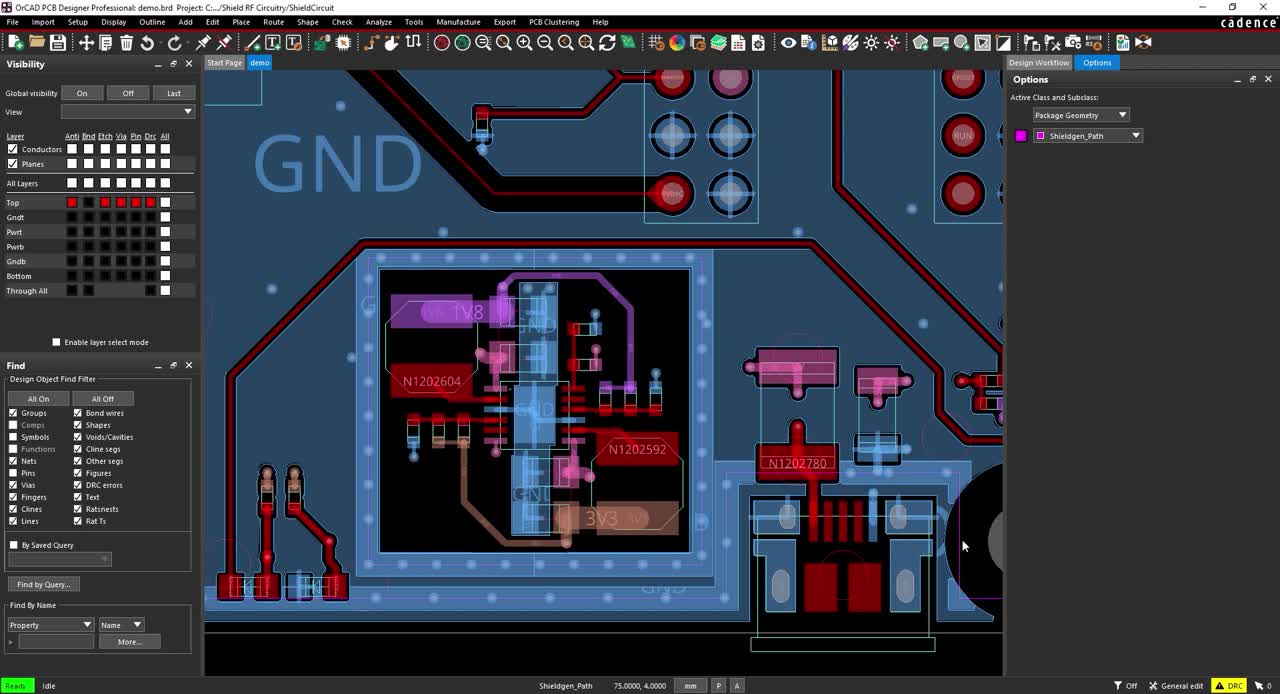
Step 1: Open the provided design, demo.brd, in OrCAD PCB Designer Professional with the Allegro Productivity Toolbox option selected.
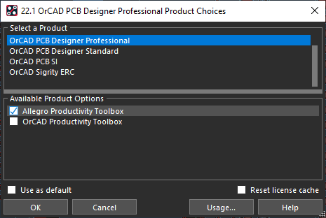
Note: Allegro Productivity Toolbox can be selected when launching OrCAD PCB Designer. To change licenses, select File > Change Editor.
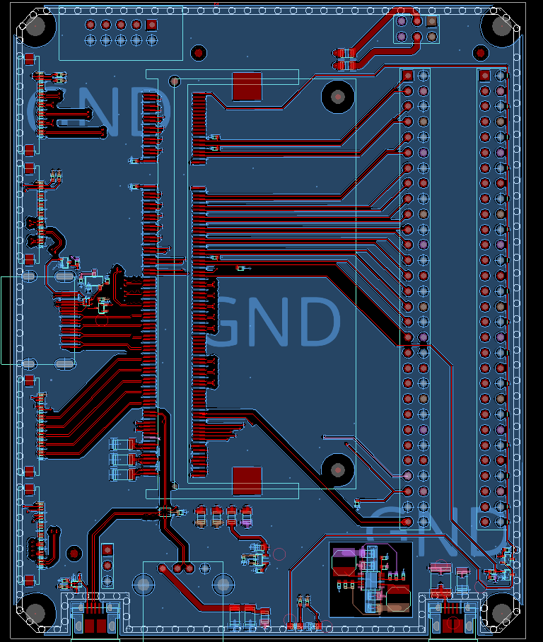
Creating a Via Shield Around the Board
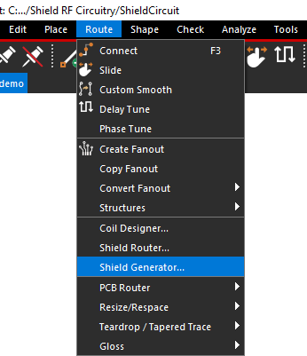
Step 2: Select Route > Shield Generator from the menu. The Shield Generator window opens.
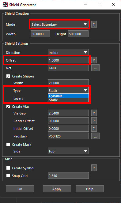
Step 3: Ensure the selected Mode is Select Boundary.
Note: In this mode, easily select a shape such as the design outline or route keepin for the shield to be created along.
Step 4: Set the offset to 1.5.
Note: This specifies the clearance from the boundary to the center path.
Step 5: Under Create Shapes, set the Type to Dynamic.
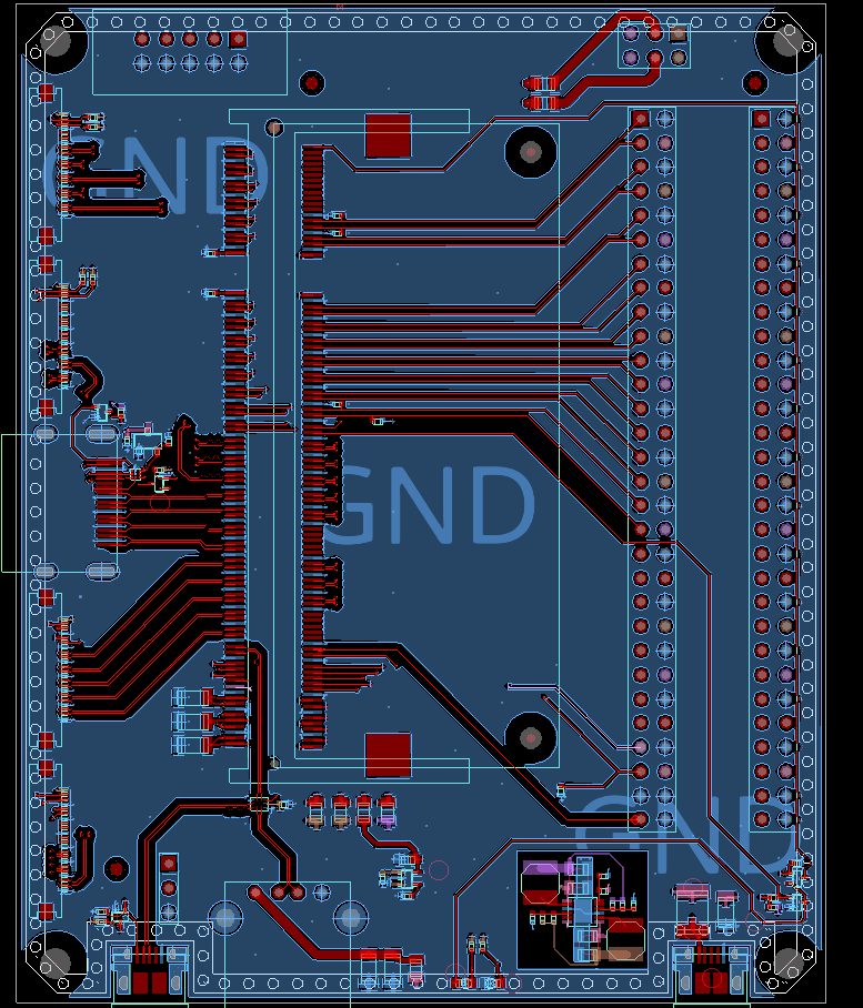
Step 6: Select the ground shape to create a preview of the shield.
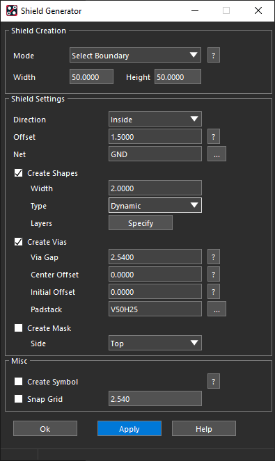
Step 7: Select Apply.
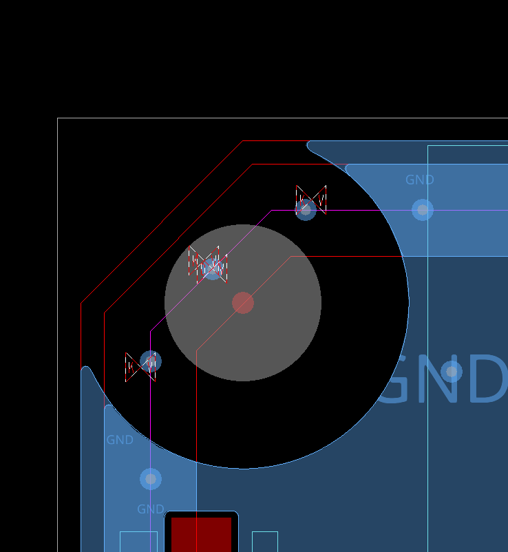
Note: The shield has been created but it is interfering with the PCB layout as noted by the design rule check errors.
Modifying a Via Shield
Step 8: Under Mode, select Delete Shield.
Step 9: Click the shield on the PCB canvas to delete it.
Step 10: Under Mode, choose Select Boundary.
Step 11: Change the Offset to 1.0.
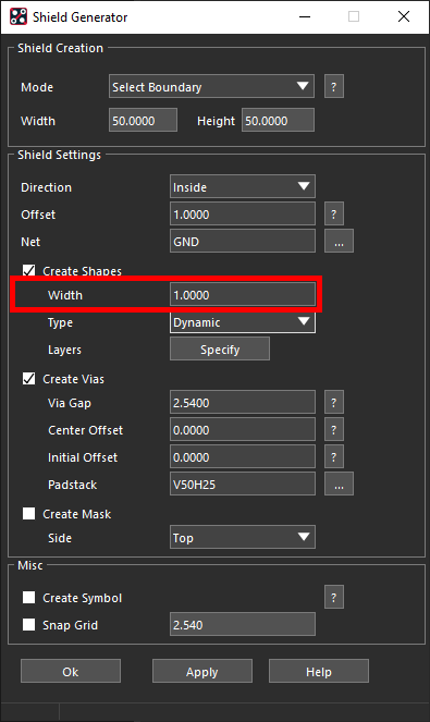
Step 12: Set the Width to 1.0.
Step 13: In the PCB canvas, select the ground shape to create a preview of the shield.
Step 14: Select Apply.
Step 15: Under Mode, select Delete Shield Via.
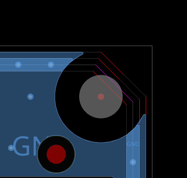
Step 16: In the PCB Canvas, click the shield vias in each corner of the PCB, the shield vias that interfere with the connectors towards the bottom of the PCB, and any other vias creating DRC errors.
Note: If a shield via was deleted unintentionally, select Add Shield Via as the mode. Click to place the via in the desired location on the PCB.
Step 17: Due to the via gap, some vias may need to be added for optimal shielding. From Mode, select Add Shield Via.
Step 18: Click the desired location on the shield to add a via.
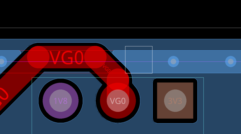
Creating a Via Shield for Specific Circuitry
Step 19: Under Mode, select Draw Rectangle.
Note: This mode allows you to draw a rectangle on the PCB canvas to shield specific circuitry.
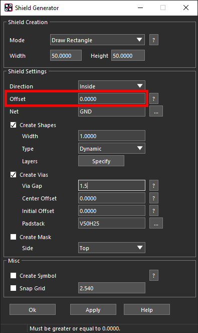
Step 20: Set the Offset to 0.
Step 21: Set the Via Gap to 1.5.
Note: This setting dictates the space between vias, center to center, around the path.
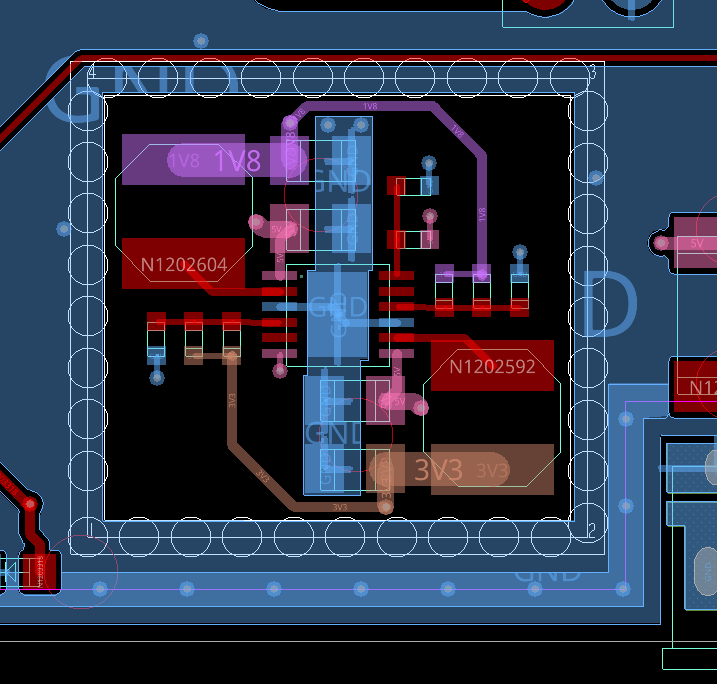
Step 22: In the PCB canvas, click and drag a rectangle around the desired block of circuitry.
Step 23: Select Apply and OK.
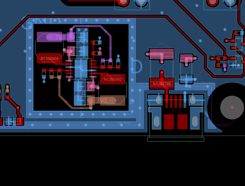
Step 24: View the created shield.
Wrap Up & Next Steps
Efficiently create the required via shielding in OrCAD to prevent EMI and noise from effecting design performance with Shield Generator in Allegro Productivity Toolbox. To learn more about the time-saving features included in the OrCAD and Allegro Productivity Toolbox, view this on-demand webinar.

