

As PCB designs continue to push the limits of speed, density, and complexity, routing high-speed signals has become one of the most critical aspects of successful board development. Signal integrity challenges such as skew, crosstalk, impedance discontinuities, and timing mismatches can often be traced back to routing decisions made long before the first trace is placed.
Effective high-speed PCB routing begins with planning. Rather than treating routing as a task that starts after component placement, experienced designers establish a routing strategy early in the design process. Allegro X offers two key techniques, flow planning and net bundling, to help teams plan routing on a PCB by visualizing signal paths, organizing related interfaces, and identifying potential routing bottlenecks before layout begins.
This quick how-to will provide step-by-step instructions on how to plan routing on a PCB with bundles and flow planning in Allegro X.
To follow along, download the provided files above the table of contents.
How-To Video
 Open in New Window
Enabling the Ratsnest Lines
Step 1: Open the provided design in Allegro X PCB Designer.
Step 2: All ratsnest lines in the design are turned off. To enable the lines for the nets that will be bundled, select Display > Show Rats > Net from the menu.
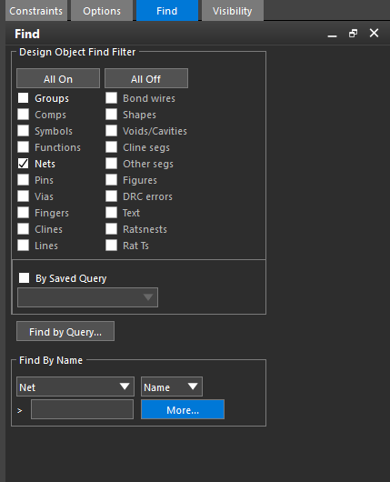
Step 3: In the Find panel, under Find By Name, select More to define the nets.
Step 4: The Find by Name or Property window opens. In the Name Filter field, enter HDMI* to filter the HDMI nets.
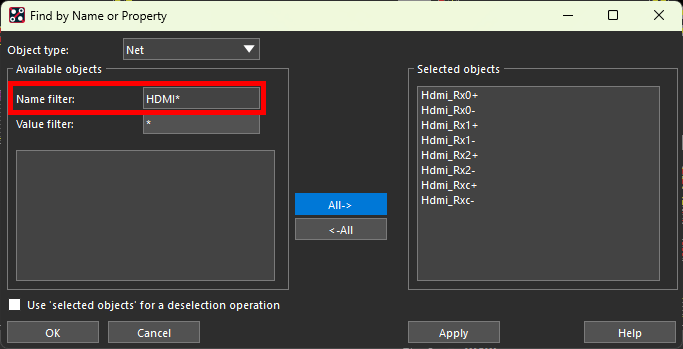
Step 5: Select All-> to select all HDMI nets.
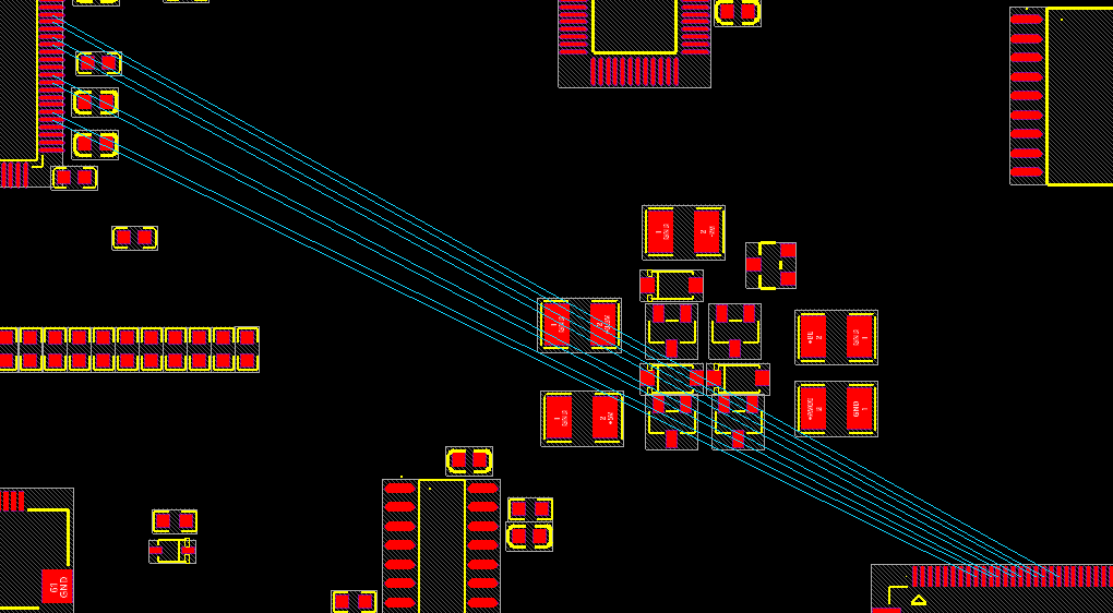
Step 6: Click OK. The ratsnest lines are enabled and displayed in the PCB canvas.
Step 7: Right-click and select Done to end the selection mode.
Plan Routing on a PCB: Creating a Bundle
Step 8: To plan routing on a PCB, flow planning settings are enabled in the Flow Planning application mode. Select Setup > Application Mode > Flow Planning from the menu to change the mode to Flow Planning.
Note: Alternatively, right-click and select Application Mode > Flow Planning or select the mode from the selection menu at the bottom of the window.
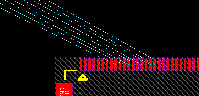
Step 9: Bundles can be used to plan the paths for ratsnest lines between components in this design. Ensure Ratsnests is checked in the Find panel then click and drag to select the ratsnest lines.
Step 10: Select FlowPlan > Create Bundle from the menu to create the bundle.
Step 11: The bundle visibility is off by default. Select the Color icon from the toolbar to enable it.
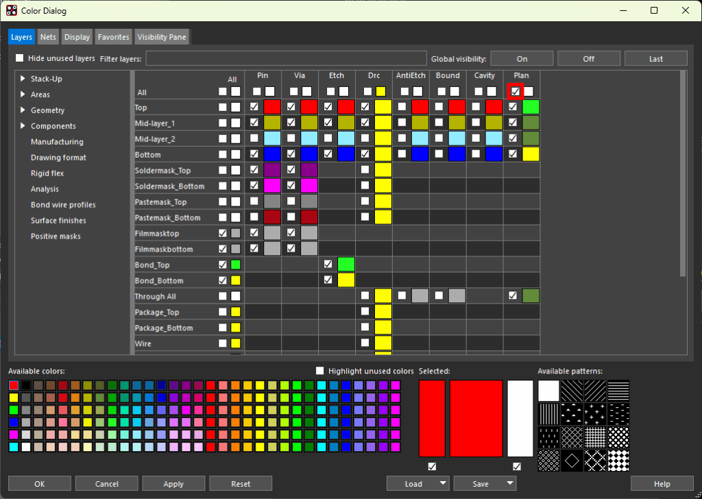
Step 12: In the Color Dialog window, check the option for All under Plan to enable bundle visibility.
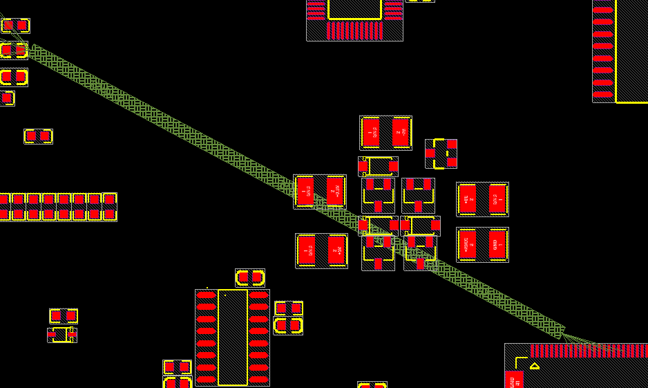
Step 13: Click OK to save the changes and close the window. The bundle is now visible between FPC1 and U18. The ratsnest lines start and end at the bundle, so the view is much cleaner.
Plan Routing on a PCB: Configuring Bundle Properties
Step 14: By default, the bundle is shown at 50% of the total width of the enclosed nets. To change this, select Setup > Design Parameters.
Step 15: The Design Parameter Editor window opens. Select the Flow Planning tab.
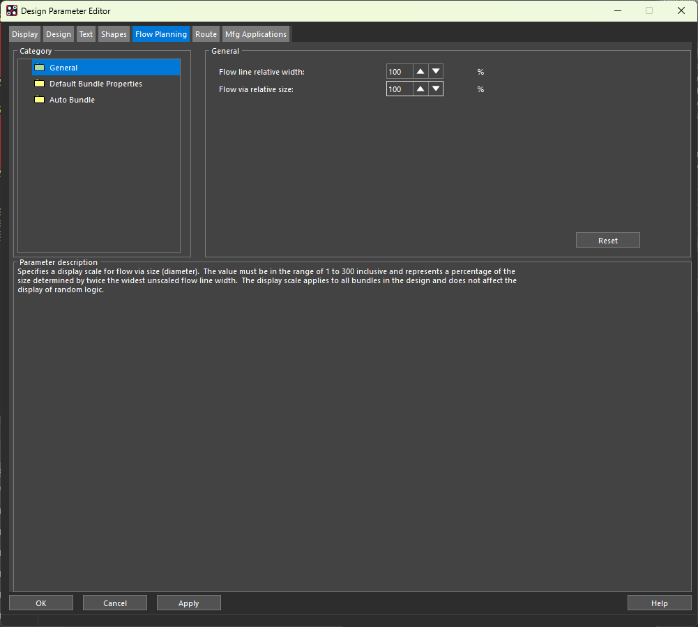
Step 16: Set the Flow Line Relative Width to 100 and the Flow Via Relative Size to 100. The bundle will now be shown at the full combined width of the enclosed nets. Click OK to save the settings and close the window.
Step 17: Select the bundle. Right-click and select Bundle Properties.
Step 18: The Edit Bundle Property window opens. Here you can configure the bundle name, ownership, and display controls. Enter BNDL_HDMI for the Bundle Name.
Step 19: Select the Bundle Layer tab. The layers to be shown in the bundle are listed.
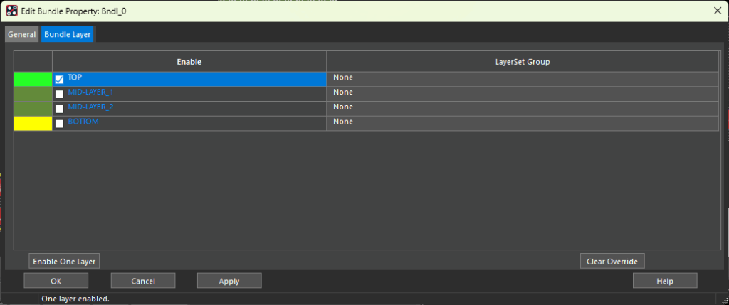
Step 20: Select Enable One Layer and choose TOP in the Enable column. TOP is selected as the only visible layer.
Step 21: Click OK to save the settings and close the window.
Adjusting the Bundle
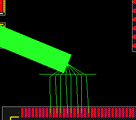
Step 22: Click and drag the start of the bundle at the flex connector to center it in the clear path between the connector and U18. A guide is shown where the ratsnest lines enter the bundle.
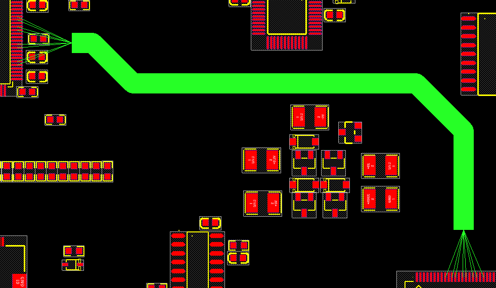
Step 23: Click and drag other points in the bundle to wrap the bundle around the path. The remaining ratsnest lines follow the path of the bundle.
Routing Bundled Traces
Step 24: To route the bundled ratsnest lines, select Route > Connect from the menu.
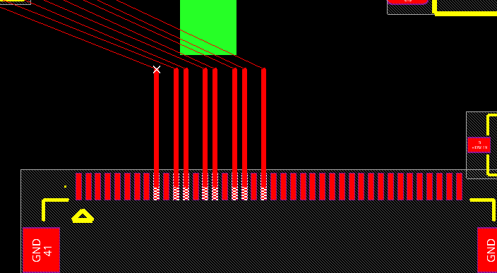
Step 25: Click and drag to select the ratsnest lines to begin routing. Traces will be routed from all selected pins.
Step 26: Eight traces are attached to the cursor. Right-click and select Route Spacing.
Step 27: The Route Spacing window opens. Select Minimum DRC for the Spacing Mode and click OK.
Step 28: Click to start routing. The traces are now closer together.
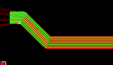
Step 29: Click to route the traces along the path of the bundle. The bundle makes for a clear and easy path for the traces to follow.
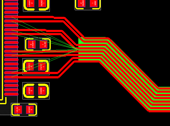
Step 30: Right-click and select Finish to automatically route the traces to their respective pins. Right-click and select Done.
Step 31: If any spacing DRC markers appear, select Route > Slide from the menu and click the traces to adjust them and clear the errors.
Step 32: The bundle and associated ratsnest lines are still visible in the PCB canvas. Right-click the bundle and select Delete Bundle to remove them. The traces are routed and the ratsnest lines are gone.
Step 33: Right-click in the canvas and select Application Mode > General Edit to return to the General Edit mode.
Wrap Up & Next Steps
Plan routing on a PCB by mapping signal flow across the board and grouping critical nets into logical bundles with Allegro X to create cleaner routing channels, reduce layer transitions, and improve overall signal performance. Get more how-tos for Allegro X at EMA Academy.

