When a board is complete and the design is ready for manufacturing, the next step is to create digital artwork films for all layers on the board to send to your fabricator. In the past, this was a tedious and time-consuming process, especially for large boards consisting of several layers. New in OrCAD X PCB Designer 24.1 is the ability to quickly generate artwork film records by selecting the layers required for artwork films and generating the film records in a single step.
This quick how-to will provide step-by-step instructions on how to quickly generate artwork film records in OrCAD X PCB Designer.
To follow along, download the provided files above the table of contents.
To learn how to generate artwork film records in OrCAD X Presto, see our how-to here.
How-To Video
 Open in New Window
Activate the Artwork Control Form
Step 1: Open the provided design in OrCAD X PCB Designer 24.1.
Step 2: Select Export > Gerber from the menu. The Artwork Control Form window opens.
Defining the Gerber Output

Step 3: The Artwork Control Form window shows a list of loaded films and properties for the selected film. Currently, only conductor films are present.
Select the General Parameters tab.
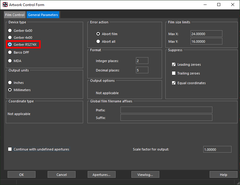
Step 4: Under Device Type, select Gerber RS274X.
Step 5: Click Film Control to return to the Film Control subpanel.
Generate Artwork Film Records: Defining Default Settings
Step 6: Select Config under Available Films to configure the films to be generated.
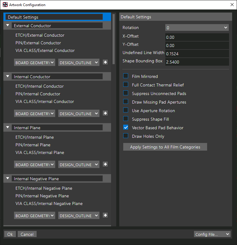
Step 7: The Artwork Configuration window opens, showing a list of new films. A default set of films has been defined.
Select Default Settings to configure the default film settings.
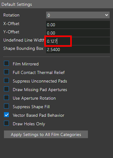
Step 8: Enter 0.127 for the Undefined Line Width.
Note: Be sure to consult with your PCB manufacturer for required line widths and specifications.
Generate Artwork Film Records: Defining Films
Step 9: Scroll down to the section labeled Silkscreen to adjust the silkscreen settings.
Step 10: The two subsections under Silkscreen are labeled as SSTP and SSBT. Rename these to Silkscreen Top and Silkscreen Bottom, respectively.
Step 11: Both silkscreen layers need a design outline subclass for reference. Select Board Geometry and Design Outline from the class and subclass dropdowns at the bottom of the list for Silkscreen Top.
Step 12: Click the + sign to add the layer.
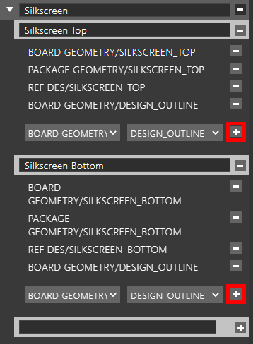
Step 13: Repeat steps 11-12 for Silkscreen Bottom.
Step 14: Scroll down to the Soldermask section to adjust the solder mask settings.
Step 15: Change the names for SMTP and SMBT to Soldermask Top and Soldermask Bottom.
Step 16: Select Board Geometry and Design Outline from the dropdowns at the bottom of the list for Soldermask Top.
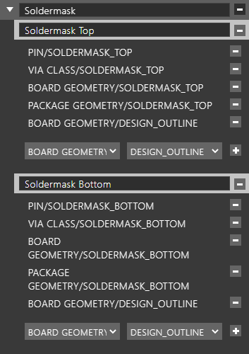
Step 17: Click the + sign to add the layer. Repeat steps 16-17 on Soldermask Bottom.
Step 18: Scroll down to the Solderpaste section to adjust the paste mask settings.
Step 19: Change the names for SPTP and SPBT to Solderpaste Top and Solderpaste Bottom.
Step 20: Select Board Geometry and Design Outline from the dropdowns at the bottom of the list for Solderpaste Top.

Step 21: Click the + sign to add the layer. Repeat steps 20-21 on Solderpaste Bottom.
Step 22: Scroll down to the Fabrication Drill Views section. Select Manufacturing and XSection_Chart from the class and subclass dropdowns at the bottom of the section. Click the + sign to add the layer.
Step 23: Scroll down to the Assembly Drawing Views section. Rename ASSYTP and ASSYBT Assembly Top and Assembly Bottom.
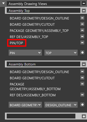
Step 24: Select Pin and Top from the class and subclass dropdowns for Assembly Top and click + to add the layer.
Step 25: Select Pin and Bottom from the class and subclass dropdowns for Assembly Bottom and click + to add the layer.
Saving a Configuration File
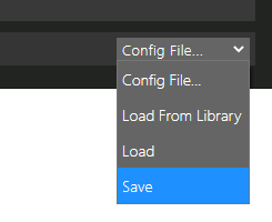
Step 26: Configuration files can be saved for quick recall for future designs. Open the Config File dropdown at the bottom of the window and select Save.
Step 27: The file browser opens to save a JSON file. Enter artwork_film_records for the name and click Save. The configuration file is saved and can be used in a later board design.
Note: In future designs, this configuration file can be loaded for automatic definition of the artwork views by selecting Config File > Load in the Artwork Configuration window. For the configuration file to be applicable, the layer stackup must be the same.
Step 28: Click OK to close the Artwork Configuration window.
Generate Artwork Film Records
Step 29: A prompt appears that the artwork film configuration has been changed and film records must be re-generated. Click Yes to generate the film records.
Note: Select Generate Films in the Artwork Control Form window to re-generate the film records as required.
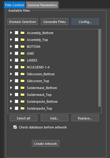
Step 30: View the list of available films. The list contains the original conductor layers plus the layers added earlier in the how-to.
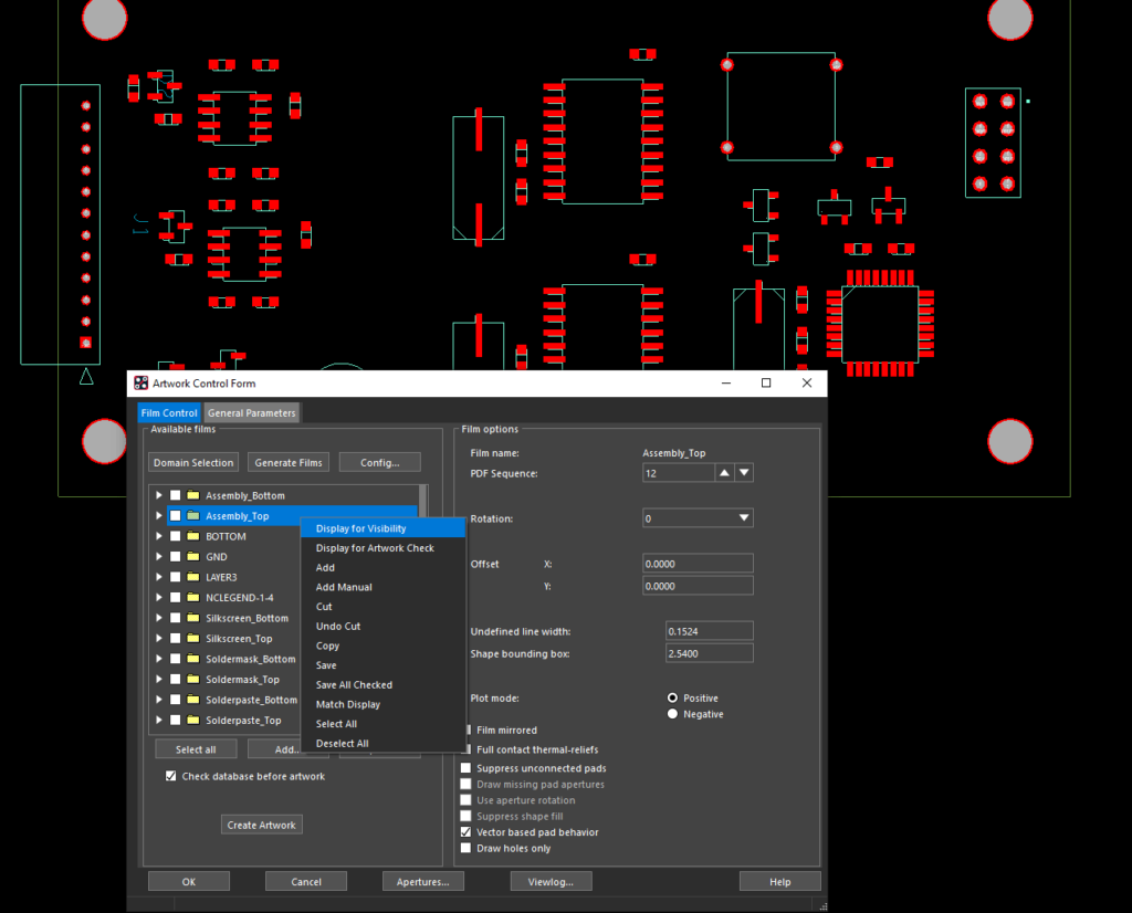
Step 31: Right-click the Assembly_Top film and select Display for Visibility. The canvas view is adjusted to show the Assembly_Top film as defined in the configuration.
Creating Artwork
Step 32: Before the artwork Gerber can be generated, the save location must be defined. With the Artwork Control Form window open, select Setup > User Preferences from the menu.
Step 33: Select File Management > Output Dir from the Categories sidebar.
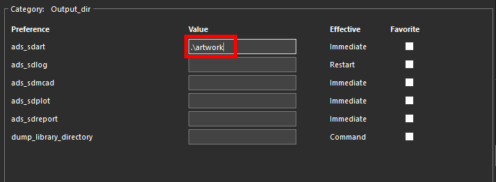
Step 34: Enter .\artwork into the ads_sdart field to define the artwork path. Click OK.
Step 35: Back in the Artwork Control Form window, choose Select All to select all films for artwork generation.
Step 36: Click Create Artwork to start generating artwork.
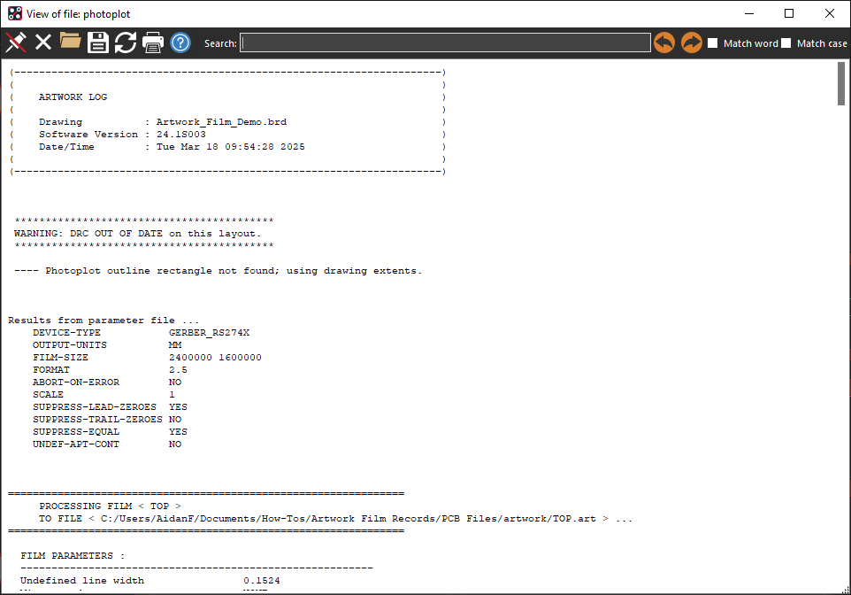
Step 37: When generation is finished, a log file opens to show the apertures used and the location of each artwork file. View and close the file.
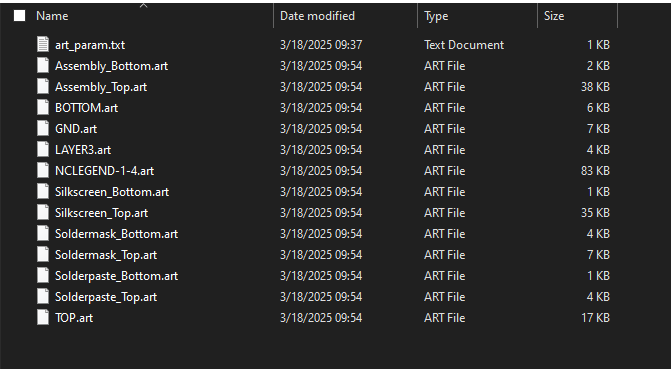
Step 38: Open File Explorer and browse to the working directory. The Artwork folder has been created. Open the folder to see the generated files.
Wrap Up & Next Steps
Quickly generate artwork film records with easy definition and configuration using the new Artwork Control Form in OrCAD X PCB Designer 24.1. Test this feature and more with a free trial of OrCAD. Get more how-tos for OrCAD X at EMA Academy.

