The key to success with any circuit is a solid connection to power and ground, typically made through power and ground planes on otherwise unused layers of the board. While there are several methods available to create planes manually, designers can use AI to generate power planes for PCB layout and accelerate the design process with Allegro X AI in OrCAD X.
This quick how-to will provide step-by-step instructions on how to use AI to generate power planes and ground planes with X AI in OrCAD X.
To follow along, download the provided files above the table of contents.
How-To Video
 Open in New Window
Starting X AI
Step 1: Open the provided design in OrCAD X.
Step 2: Select Tools > X AI from the menu to open the X AI panel. This panel can be docked or undocked and moved anywhere in the canvas.
Step 3: Select Login and enter your Cadence username and password.
Step 4: Select Create New Workspace at the top of the Workspaces panel.
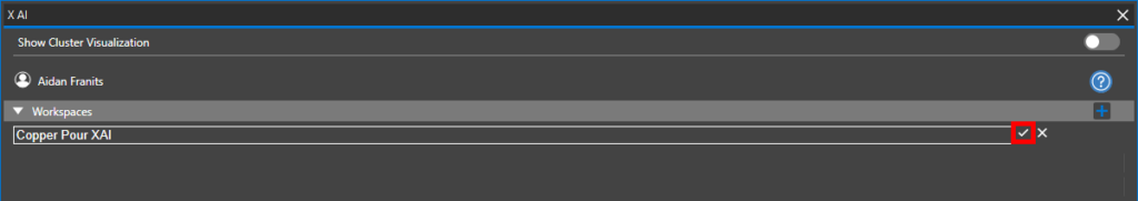
Step 5: Enter a name for the new workspace and click the checkmark button to create it.
Step 6: In the main workspace window, select Upload Board to upload the currently-loaded board to the X AI server.
Configuring Component Classes
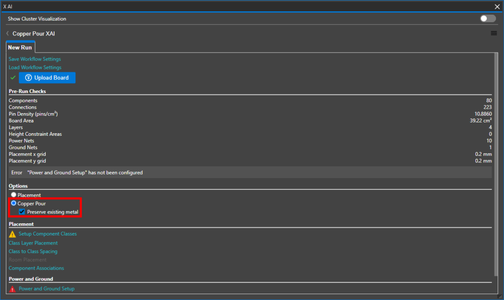
Step 7: In the X AI window, under Options, select Copper Pour and check Preserve Existing Metal to prepare for a copper pour simulation and avoid deleting any existing wiring.
Step 8: Component classes and power-ground layers must be configured properly before power planes can be drawn. Select Setup Component Classes to define unassigned component classes.
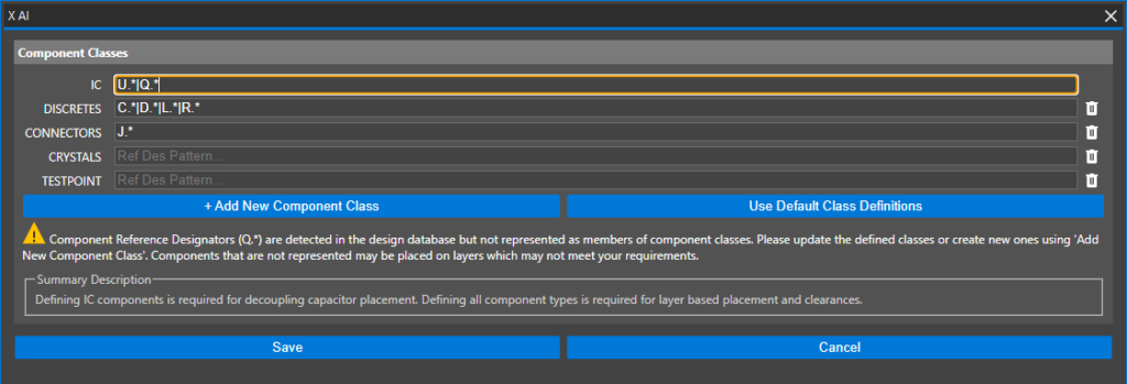
Step 9: The Component Classes panel opens with a warning message that reference designator Q.* is not defined. Add |Q.* to the IC field to define transistors as ICs.
Step 10: Click Save to save the changes and return to the main X AI window.
Defining Power and Ground Rules
Step 11: Power and ground placement rules must be defined before any planes are generated. Select Power and Ground Setup.
Step 12: The Power and Ground Setup table opens. For this design, power and ground net voltages have already been assigned and are listed in the Voltage row.
A prompt is shown, saying that power and ground settings were pre-populated from the design. Click OK to close the prompt.
Note: Power and ground nets have been automatically populated in X AI due to the pre-configuration in the Constraint Manager.
Learn more about how to configure constraints for X AI here.
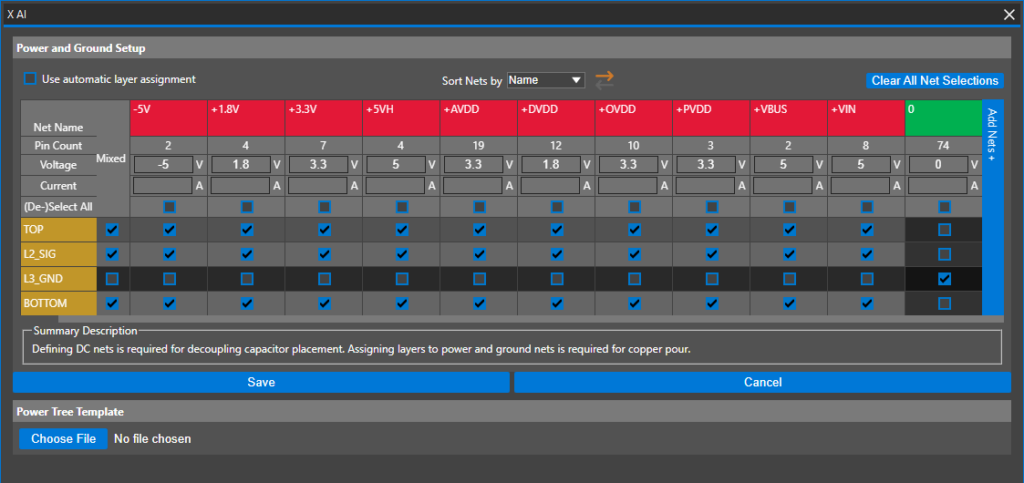
Step 13: Check the options for layers TOP, L2_SIG, and BOTTOM for all power nets and layer L3_GND for the ground net.
Note: This will allow power planes to be drawn on the TOP, signal, and BOTTOM layers, and only allow the ground plane to be drawn on the GND layer. Learn more about the settings required to get the most out of AI in your PCB layouts here.
Step 14: Click Save to save the settings and return to the main X AI window.
Use AI to Generate Power Planes for PCB Layout
Step 15: With component classes, spacing rules, and power/ground layers defined, copper planes are ready to be generated. Select Run X AI to start the pour. The Results tab opens, showing a log of the progress.
Step 16: When placement finishes, a green checkmark and a download icon are shown in the run row in the Results table. Click the download icon to download and view the board.
Note: If prompted to save the changes to the existing board, click No.
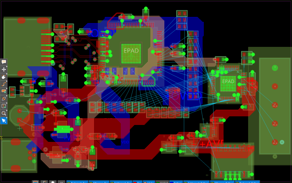
Step 17: View the generated board. Copper planes were generated for each power net on the top, signal, and bottom layers; and a ground plane was generated on the GND layer.
Note: To turn off the GND layer and make the signal layers more visible, select L3_GND from the Layer Toolbar.
Wrap Up & Next Steps
Use AI to generate power planes for PCB layout and quickly meet the demands of your power delivery network with X AI in OrCAD X. Learn more about X AI here and get more how-tos for OrCAD X at EMA Academy.

