With today’s designs growing more compact, it’s not uncommon to have as many as a dozen layers on a PCB for power, ground, and signal nets. Having signals on adjacent layers, however, can introduce crosstalk into the circuit, potentially degrading signal integrity. Adjacent power and ground planes can also introduce unintended capacitance, which, in some cases, is not desirable. New in OrCAD X PCB Designer 24.1 is the ability to quickly and easily create void shapes in adjacent layers for optimal power and signal integrity.
This quick how-to will provide step-by-step instructions on how to void shapes in adjacent layers in OrCAD X PCB Designer.
To follow along, download the provided files above the table of contents.
How-To Video
 Open in New Window
Activating Shape Void
Step 1: Open the provided design in OrCAD X PCB Designer.
Step 2: Select Shape > Void Adjacent Layer Shape from the menu.
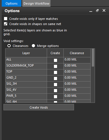
Step 3: View the Options panel. The panel is now populated with settings for adjacent shape voiding. Here you can define which layers the void is created on, whether or not to create voids in same-net planes, and whether or not to create voids on only matching layers.
Configuring Void Settings
Step 4: In the Void Settings table, check Create for GND_2to create a void in the GND_2 layer, which is directly below the TOP layer. The layer is highlighted in green in the Void Settings table.
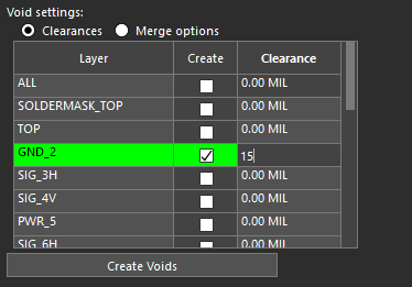
Step 5: Enter 15 mil for the GND_2 clearance.
Note: This will pad the void to be 15 mils from the shape itself.
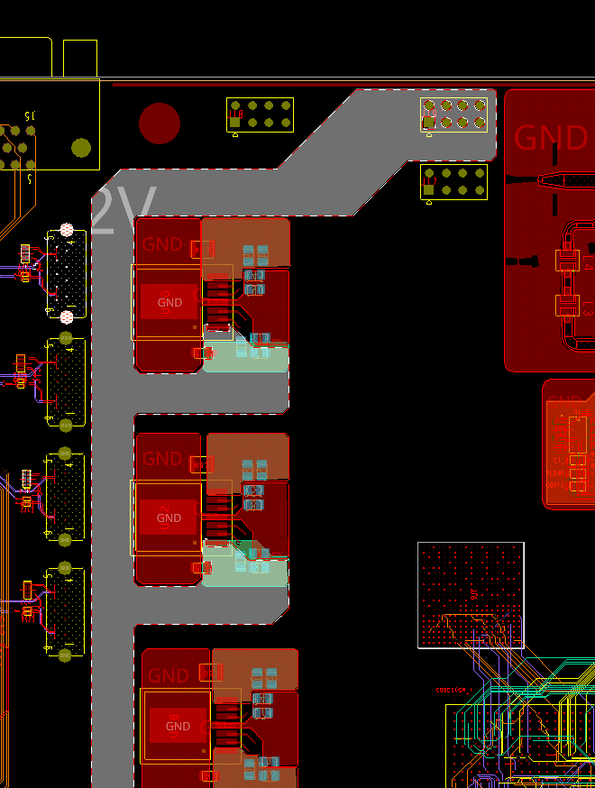
Step 6: Check Shapes in the Find panel and click the large +12V shape on the TOP layer to select it for a void reference.
Note: The TOP layer is highlighted in blue in the Void Settings table.
Create Void Shapes in Adjacent Layers
Step 7: In the Visibility panel, check the option for All for layer Gnd_2 so the layer the void will be created in is visible.
Step 8: Select Create Voids in the Options panel. A void is visible around the +12V shape.
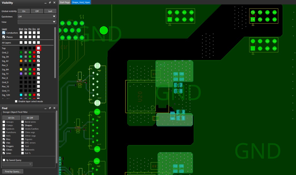
Step 9: Uncheck All for the TOP layer in the Visibility panel. The void created by the 12V shape is clearly visible in the GND_2 layer.
Check All again to re-enable visibility for the top layer.
Merging Voids
Note: If the objects whose adjacent areas are to be voided are close, the voids can be merged to prevent stray copper antennas.
Step 10: Select Merge Options under Void Settings to view the Merge Options table.
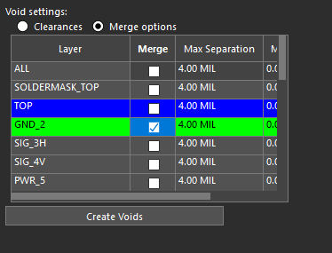
Step 11: Check the option for Merge for GND_2.
Note: Additionally, the minimum and maximum separation can be defined in this table.
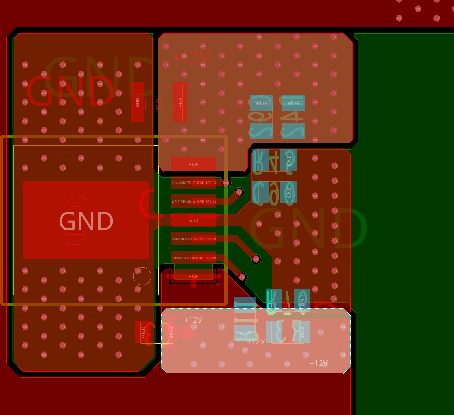
Step 12: Select the smaller +12V plane at the top of the larger plane and click Create Voids. A new void is created in the GND_2 plane, merged with the original.
Step 13: Select the +12V plane below that on layer Sig_3H. More of the GND_2 plane is voided. As before, the new void merges with the original.
Step 14: Right-click and select Done to exit the void mode.
Wrap Up & Next Steps
Quickly and easily create void shapes in adjacent layers to optimize signal and power integrity in OrCAD X PCB Designer. Test this feature and more with a free trial of OrCAD. Get more how-tos for OrCAD at EMA Academy.

