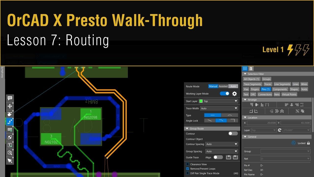
Routing
This lesson will demonstrate how to route the PCB in OrCAD X Presto, including creating fanouts, configuring net visibility, and adding vias.
To follow along, continue with the design from the previous lesson or download the starting materials from the Materials tab of this lesson.
 Open in New Window
Configuring Net Visibility and Colors
Step 1: Select Visibility to open the Visibility panel.
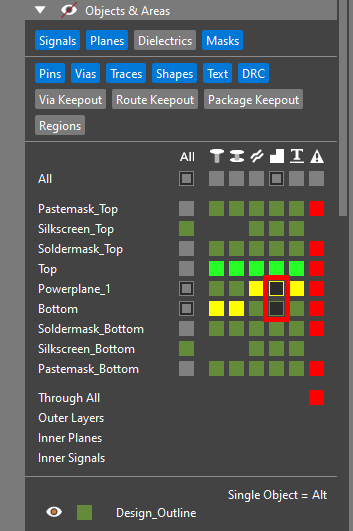
Step 2: Under Objects and Areas, in the color table, click the Shape entries for Powerplane_1 and Bottom to turn off visibility for shapes in those layers.
Note: Alternatively, hold Alt and select Top from the Floating Layer Toolbar. Only the TOP layer is visible.
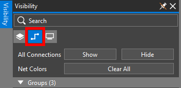
Step 3: Select the Nets mode at the top of the panel.
Step 4: Under Nets, select the color box for 3.3V.
Note: If a color is not set, a minus sign is shown in the box.
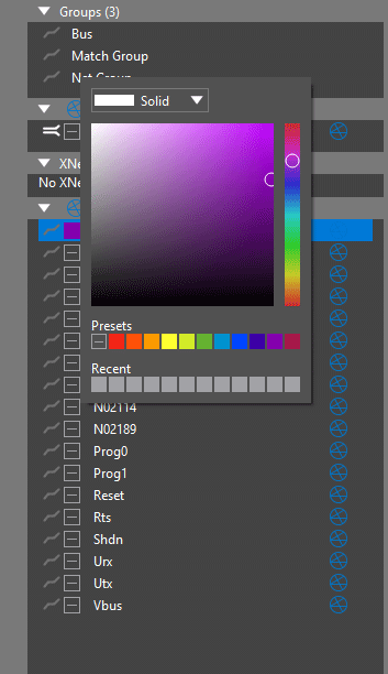
Step 5: Select Purple from the presets in the Color Selection widget. Click anywhere outside the widget to close it.
The 3.3V net is now highlighted in purple.
Step 6: Select the color box for GND.
Step 7: Select Blue from the presets in the Color Selection widget. Click anywhere outside the widget to close it. The GND net is now highlighted in blue.
Step 8: Under Diffpairs, select the color box for Dpd. Select Orange from the presets and click anywhere outside the widget to close it.
Viewing Ratsnests
Step 9: Select Hide for All Connections. This will disable all ratsnest lines.
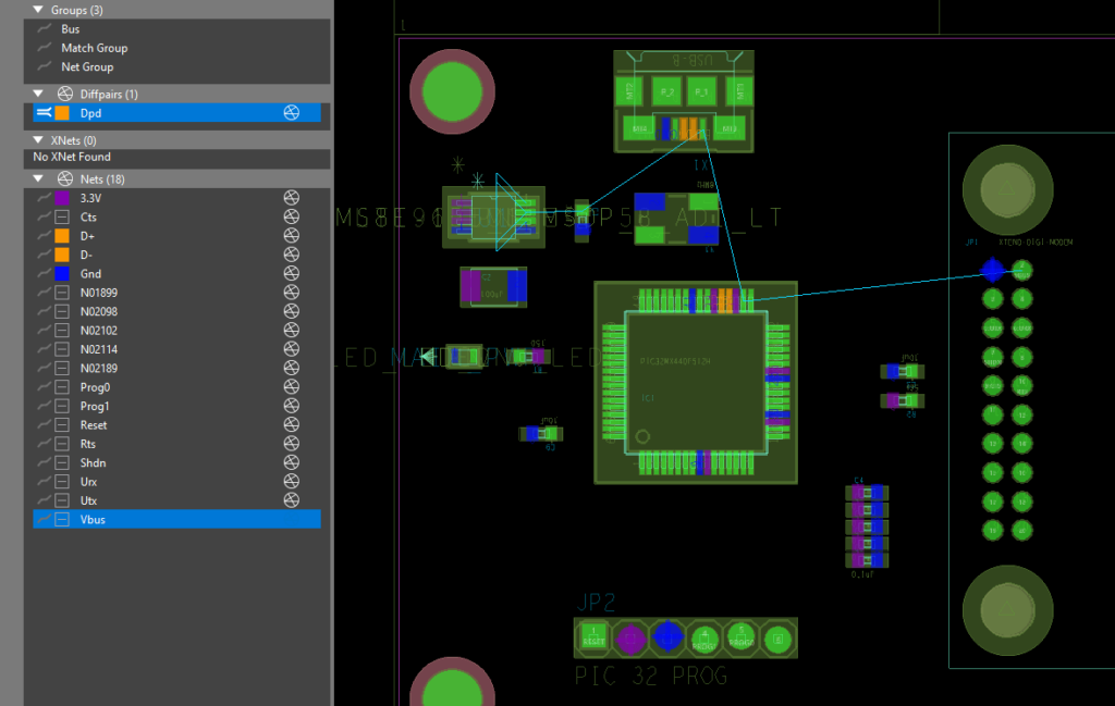
Step 10: Hold Alt on the keyboard and select the ratsnest symbol for Vbus under Nets. Only the ratsnest for net Vbus is highlighted.
Step 11: Right-click the net listing and select Select on Canvas. The net’s ratsnest lines and all pins connected to it are selected.
Step 12: Hold Alt and select the ratsnest symbol for Utx. The Vbus pins remain selected but only the ratsnest for Utx is visible.
Step 13: Select Show for All Connections. This will enable all ratsnest lines.
Step 14: Select Visibility again to close the panel and click anywhere in the canvas to deselect the net.
Creating Fanouts
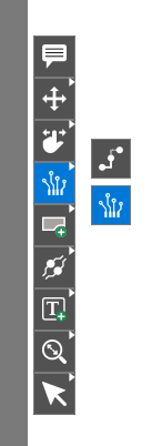
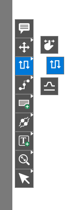
Step 15: Right-click the Add Connect mode in the toolbar and select Fanout.
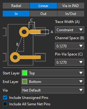
Step 16: The Fanout widget opens. Select Linear.
The fanout window lets you easily configure fanout parameters and provides a visual representation of the fanout. Fanout options include fanout type such as Radial and Via in Pad, trace width and spacing, starting and ending layers, and the via.
Note: Use the Include Unassigned Pins option to fan out pins with no defined net.
Step 17: Select Out. This will create outward-facing fanouts.
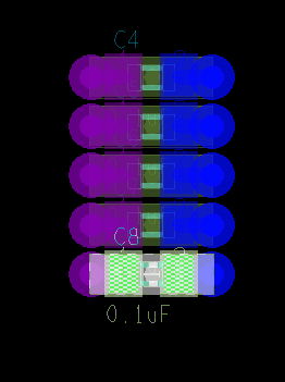
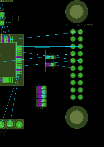
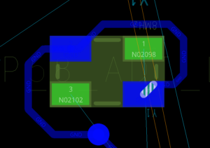
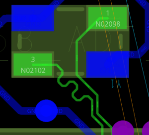
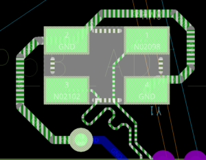
Step 18: Click C2 and C4-C8 on the canvas to create the fanouts. These capacitors each have two pins that connect to power and ground.
Step 19: In the Properties panel, under Selection Filter, select All Objects to turn all objects off, then select Pins to select only pins.
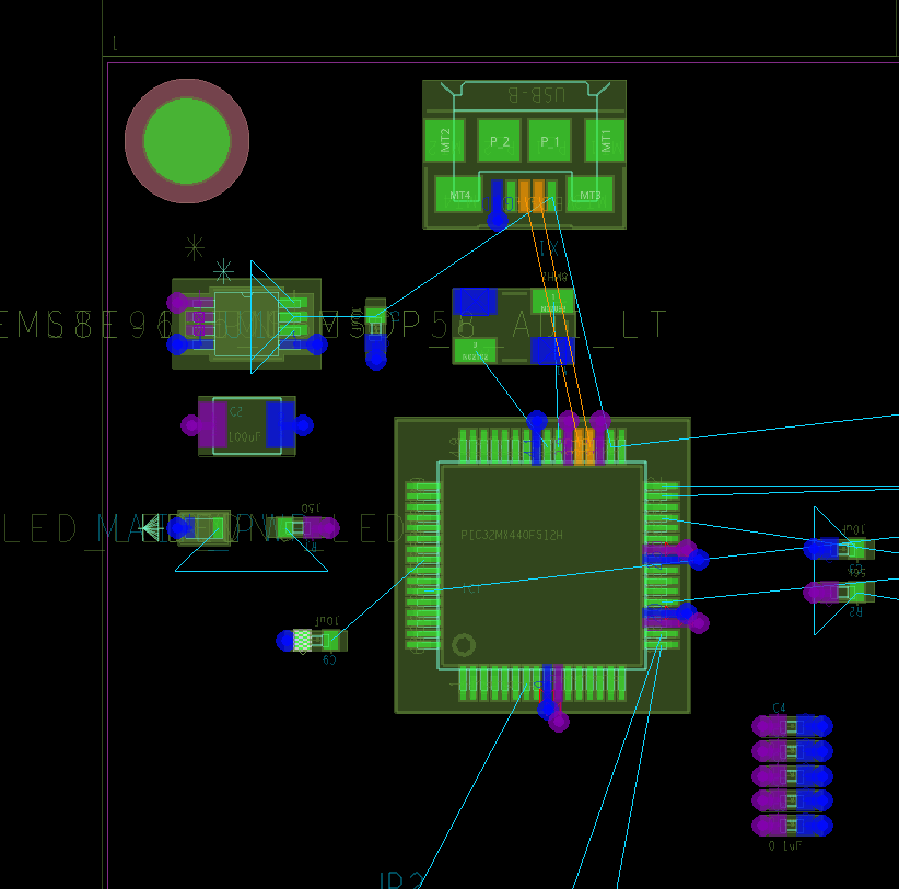
Step 20: Click the remaining power and ground pins on the design, except for the following pins:
- Both ground pins on crystal Y1
- Pins 2 and 3 on IC U1
- Any through-hole ground or power pins
The fanout is created and the pads are connected to the required power/ground.
Note: If you make a mistake, press CTRL-Z on the keyboard.
Routing the Crystal Grounds
Note: High-frequency components such as crystals often have special routing requirements.
Step 21: Select the Slide mode from the toolbar.
Step 22: Select Assisted in the resulting widget. Using an assisted slide mode will prevent traces from being moved into another pin or trace.
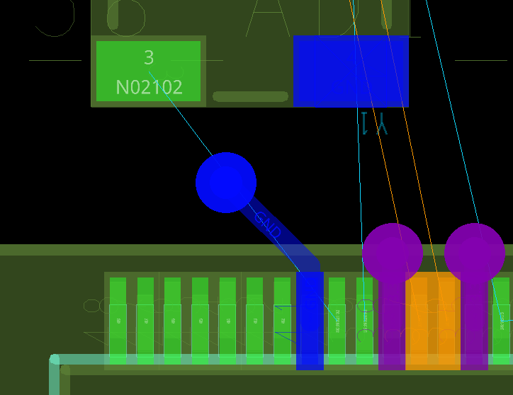
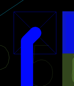
Step 23: Click to select the ground via on IC1, just below the crystal. Move the via upwards and to the left then click to place the via.
Step 24: On the toolbar, right-click the Fanout mode and select Add Connect.
Step 25: Select Assisted in the resulting widget. In the Add Connect widget, you can set:
- The trace width
- The trace angle
- Whether to hug or shove other traces and vias when routing
- Trace smoothing
- Routing Layers
Step 26: Click to draw a ground trace around the perimeter of the crystal between the via and the upper-left ground pad of the crystal.
Note: A box with an “x” appears on the trace as it’s being drawn.
Step 27: Click to draw a ground trace around the crystal between the upper-left and lower-right ground pads.
Routing the Crystal Oscillation Pins
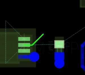
Step 28: Select the lower-left pad on Y1 to start routing a trace. Click the canvas to place the trace. A green ratsnest line connects the pads during routing.
Step 29: Click the corresponding pad on IC1 to finish the trace.
Step 30: Select the upper-right pad on Y1 to start routing a trace. Click the canvas to place the trace and click the corresponding pad on IC1 to finish the trace.
Step 31: On the toolbar, right-click the Slide mode and select Delay Tune.
Step 32: Select Assisted in the resulting widget.
Step 33: Select a section of the shorter of the two traces to start delay tuning.
Step 34: Move the cursor further outward to even out the lengths of the two nets. Click to finish the delay tune.
Note: Repeat steps 33-34 to add more delay tuning as needed.
Locking Traces
Step 35: Select the Select mode from the toolbar or press Escape on the keyboard.
Step 36: In the Properties panel, under Selection Filter, click to disable Trace Segments and click to enable Traces. This will allow you to select whole traces without having to click individual segments.
Step 37: Select Vias and Components in the same subpanel.
Step 38: Hold Ctrl and select crystal Y1, the ground and oscillation traces that connect to it, and the ground via.
Step 39: Select the lock symbol in the Properties panel to lock the objects. Click anywhere to deselect. This will prevent the objects from being moved or modified during the remainder of the PCB layout.
Routing the Remaining Traces
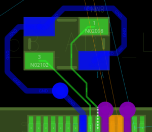
Step 40: Select the Add Connect mode from the toolbar.
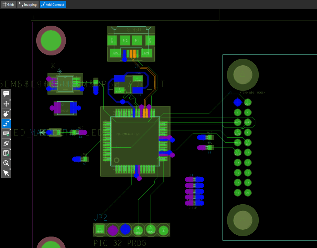
Step 41: Click the remaining pads with ratsnest lines to route the remaining traces. Complete all connections on the PCB.
Note: Ensure Pins is selected in the Properties panel under Selection Filter to easily connect to pins in the design. If you make a mistake, press Backspace on the keyboard.
Shadow Mode is available to route with only the relevant traces and pins visible at maximum brightness. To enable Shadow Mode, open the Visibility panel in the Display mode and switch Shadow Mode on. Adjust the brightness as desired.
Step 42: When routing, double-click to add a via or press V on the keyboard. The via has been added and the routing continues on the bottom layer.
Note: Available vias can be configured in the Constraint Manager. Via properties can be viewed in the Properties panel after selecting the via.
Step 43: When all connections are made, press Escape again to return to the Select mode or choose the Select mode from the toolbar. If any objects are selected, click anywhere on the canvas to deselect.
Step 44: Ensure that the Status subpanel in the Properties panel reads 0 for unrouted nets and unrouted connections.
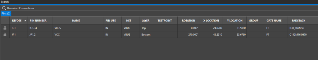
Step 45: If an unrouted net or connection is detected, click the number of unrouted connections to see which pins are unconnected in the Search pane. Activate the Add Connect mode and route the additional connections as needed.