PCB Design
How to Update Padstacks and Footprints in OrCAD X
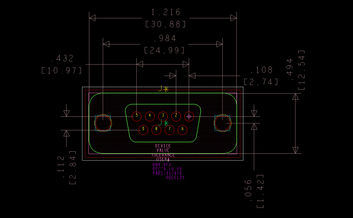
Learn how to update padstacks and footprints in OrCAD X which have been created in older versions of OrCAD PCB Designer to use in versions 23.1 and later.
Learn how to update padstacks and footprints in OrCAD X which have been created in older versions of OrCAD PCB Designer to use in versions 23.1 and later.
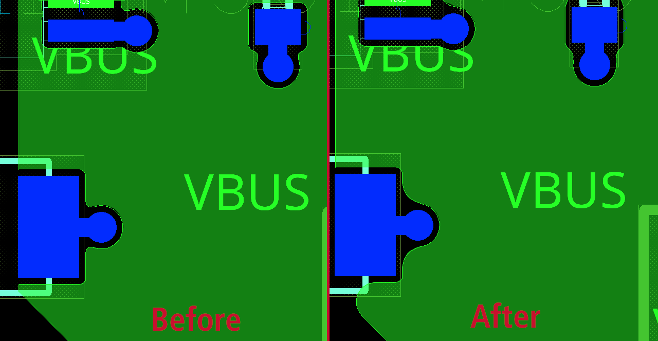
Learn how to change the fill radius of dynamic copper shapes to control sizes of shape islands and spacing around any routed traces.
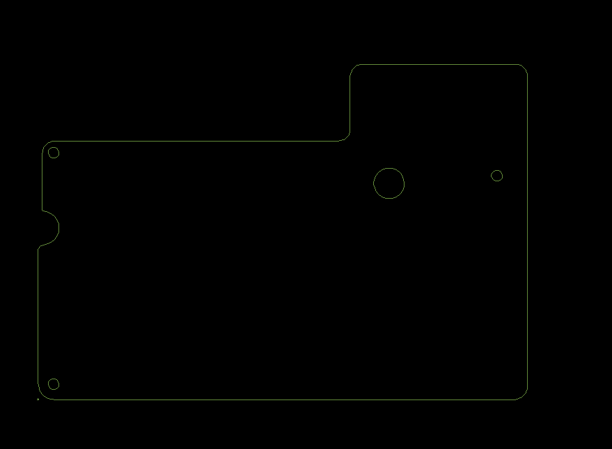
This step-by-step guide will show how to create a board outline from a DXF in OrCAD X for accurate PCB creation.
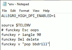
Learn how to edit the env file to assign a permanent shortcut key for all future sessions of OrCAD PCB Designer to complete PCB layouts efficiently.
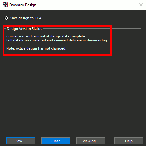
Learn how downrev a PCB file or save a board file to an earlier version of OrCAD or Allegro to increase compatibly with previous versions of the software.
Learn how to create fanouts in OrCAD for components and pins to efficiently complete your PCB layouts.
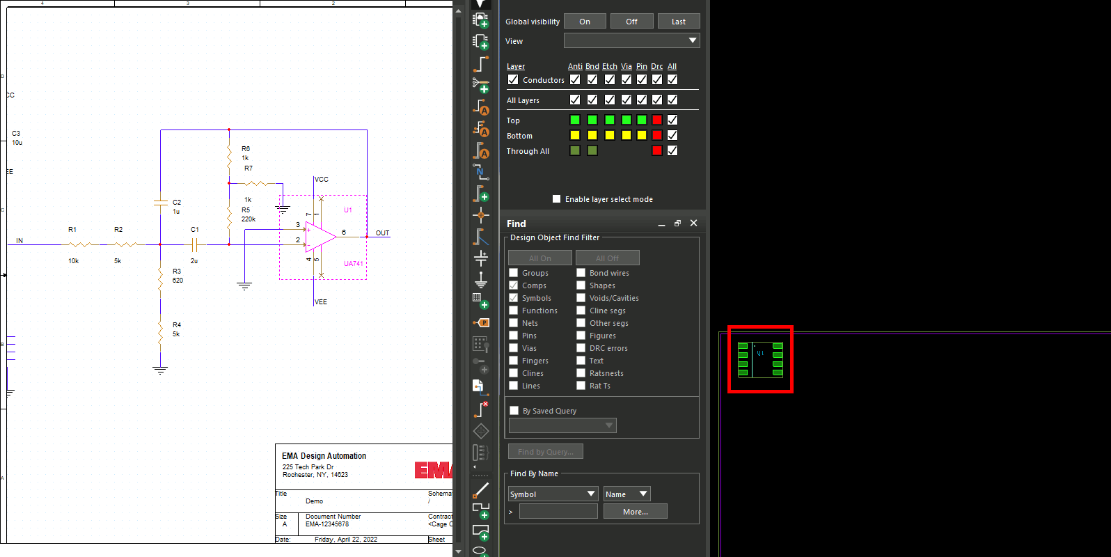
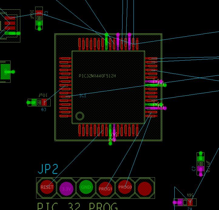
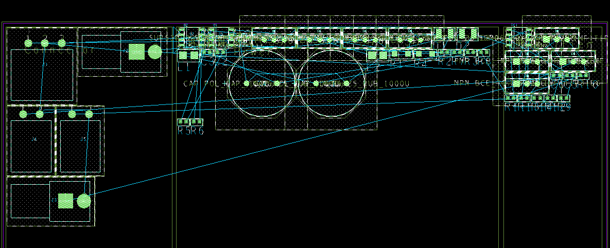
Learn how to quickly and efficiently place components on the PCB from the schematic by cross-probing in OrCAD.
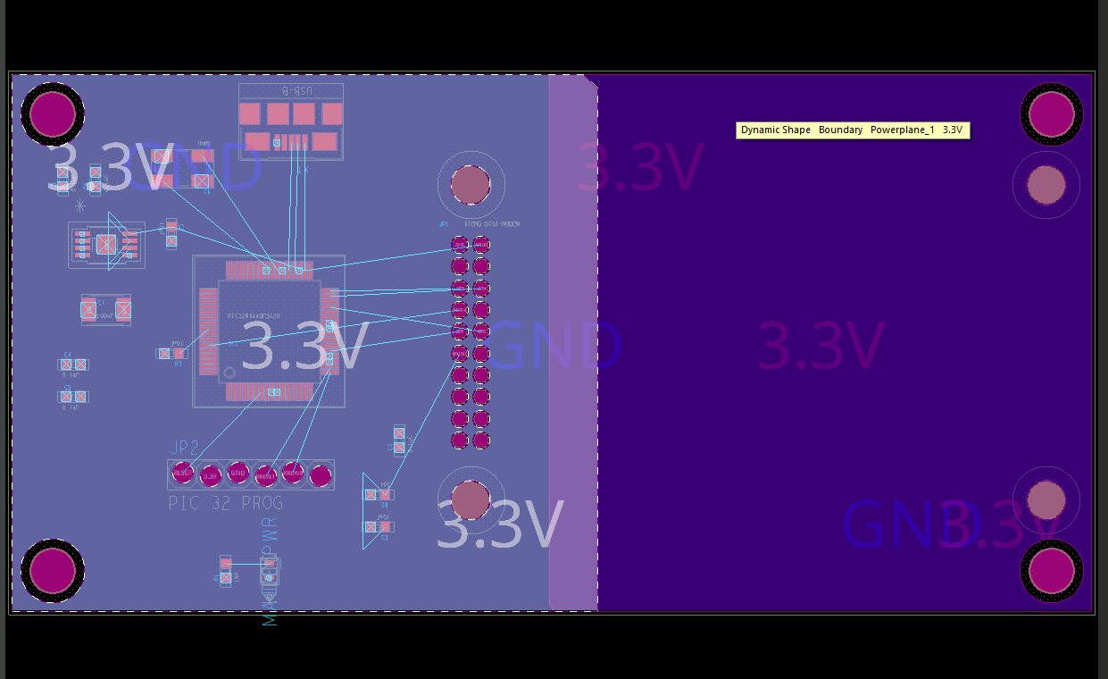
Learn how to create planes and copper pours for efficient power and ground connections in OrCAD PCB Designer.
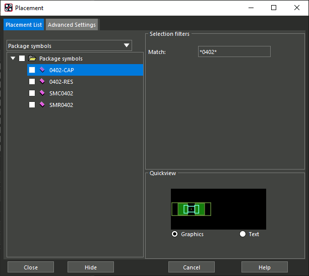
Learn how to find included PCB footprint libraries in OrCAD and browse the available symbols in OrCAD PCB Designer.
This step-by-step guide will show how to configure and create rooms for component placement for efficient PCB layout.