Define Cross Section
Location: PCB Canvas
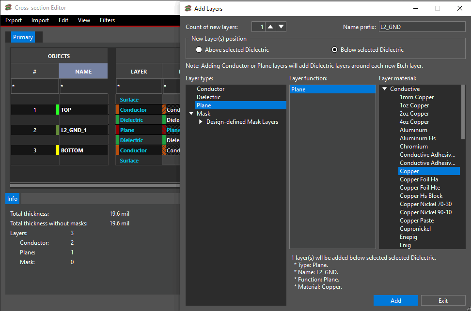
The cross-section should be created in OrCAD X or Allegro X by defining the conductor and plane layers in the PCB stackup. Additionally, all layers must have a thickness assigned. The cross-section will need to be defined in order to specify which layers should be used for copper planes and pours.
Need Help? Get the step-by-step instructions for defining your PCB stackup here: Cross Section Instructions
Completed Component Placement
Location: PCB Canvas
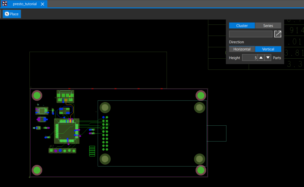
Since Allegro X AI takes component connections to power and ground into consideration when completing the copper pours, all components must be placed inside the design outline.
Define DC Net Voltage Assignments
Location: PCB Canvas
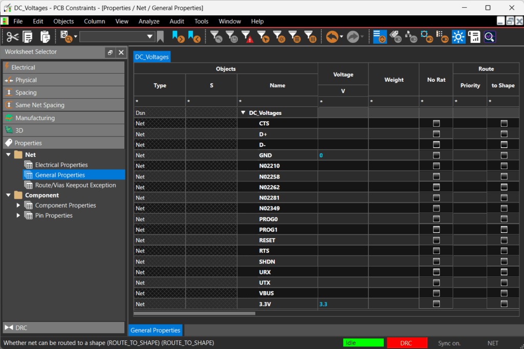
DC Voltage Nets are required. These values can be assigned in the constraint manager in OrCAD X or Allegro X, as this will automatically populate DC net names and voltage values in Allegro X AI. For copper pours in Allegro X AI, this will define the voltages that must be included in the copper pour creation.
Need Help? Get the step-by-step instructions for defining voltage levels for DC nets in the PCB here: DC Voltage Assignment Instructions
Define Physical Rules
Location: PCB Canvas
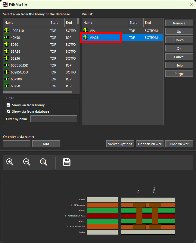
Define and assign the important physical constraints for the design in constraint manager. Allegro X AI will understand the constraints configured in constraint manager and take them into consideration when generating copper planes and pours. For copper pours, the following physical constraints should be assigned:
- Minimum line width: Define a line width that will not exceed the pin width.
- Vias: Ensure the preferred vias are selected for nets, especially power and ground nets.
Need Help? Get the step-by-step instructions for defining physical rules in the PCB here: Defining Physical Rules
Power and Ground Mapping
Location: Allegro X AI
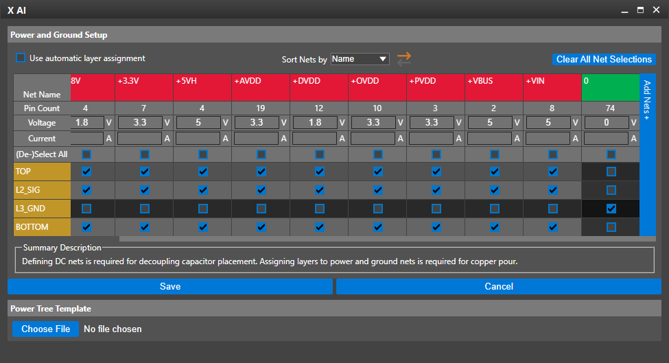
Voltage levels for power and ground must be specified and mapped by selecting Copper Pour Setup in Allegro X AI.
If DC voltage values were assigned in the constraint manager in OrCAD X or Allegro X, the power and ground nets as well as voltages will be automatically populated in Allegro X AI.
If DC voltage values were not assigned during the schematic or PCB design, select Add Nets to define the nets and corresponding voltage values.
Additionally for copper pours, the power and ground nets must be mapped to the desired layers in the cross-section. This will inform Allegro X AI which layers it can use for power and ground pours. It should also be noted if the design intent is to use the entire layer for the copper pour.
