When creating a new PCB design, the board structure must be defined as it directly impacts the design’s electrical performance, manufacturability, signal integrity, and electromagnetic compatibility. Quickly and accurately defining the right stackup is especially important with modern designs becoming more complex and project timelines shrinking. Easily add layers to a PCB stackup with OrCAD X Presto to quickly define the materials and cross-section required for your PCB designs.
This quick how-to will provide step-by-step instructions on how to add layers to a PCB stackup with the Cross-Section Editor in OrCAD X Presto.
To follow along, download the provided files above the table of contents.
How-To Video
 Open in New Window
Add Layers to a PCB Stackup: Add Layers Dialog
Step 1: Open the provided design in OrCAD X Presto.
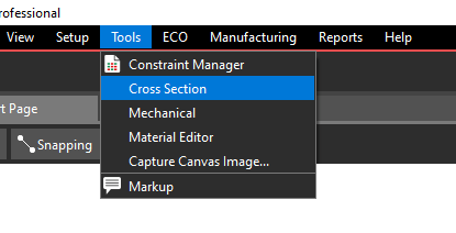
Step 2: To start the Cross-Section Editor, select Tools > Cross-Section from the menu.
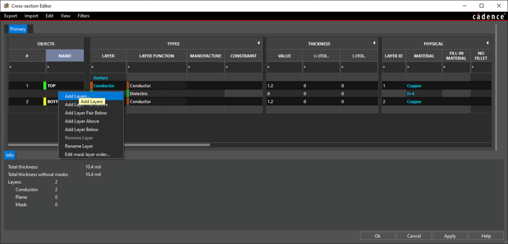
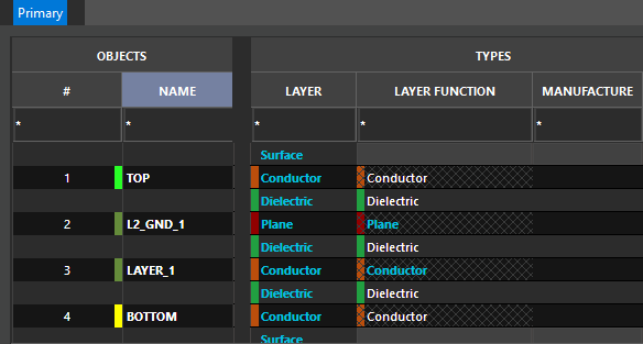
Step 3: The Cross-Section Editor opens. Here you can define all layers and stackups in the design. Currently, only the TOP and BOTTOM layers exist.
Right-click the dielectric between TOP and BOTTOM and select Add Layers.
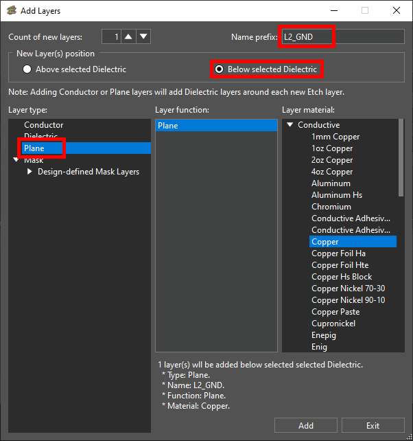
Step 4: The Add Layers window opens. Here you can define all new layer properties including type of layer, material, and position.
Enter L2_GND for the Name Prefix.
Step 5: Select Below Selected Dielectric for the layer position to place it between TOP and BOTTOM.
Step 6: Select Plane for the Layer Type. The layer function and material are automatically selected.
Step 7: Click Add to add the new ground layer. The layer is added to the stackup in the Cross-Section Editor as L2_GND_1.
Note: The dielectric below the new layer is highlighted. The Add Layers window remains open.
Step 8: Click Exit to close the Add Layers window.
Add Layers to a PCB Stackup: Cross Section Editor
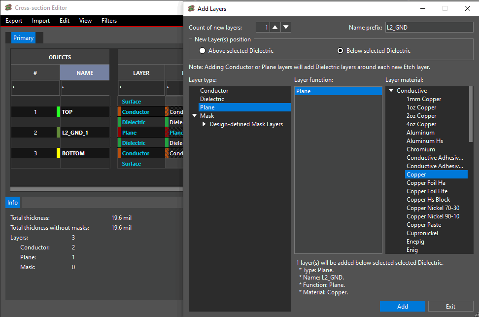
Step 9: New layers can also be created directly from the cross-section editor. Right-click the dielectric between the new plane layer and BOTTOM.
Step 10: Select Add Layer Pair Below. A new conductor layer and dielectric are added to the stackup.
Add Layers to a PCB Stackup: Layer Names
Step 11: Generally, it is good practice to name and number the layers in a stackup. Double-click L2_GND_1 in the Name column to rename the layer.
Step 12: Enter L2_GND for the name. Press Enter on the keyboard to rename the layer.
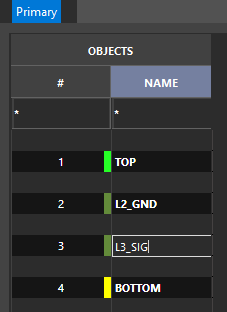
Step 13: Double-click the new conductor layer LAYER_1 and enter L3_SIG for the name. Press Enter.
Step 14: The cross section is defined. Click OK to save the changes and close the window.
Add Layers to a PCB Stackup: Layer Colors
Step 15: By default, all new layers are shown in dark green. To help distinguish the new layers during routing, assigned colors can be changed. Select Visibility from the left side of the window.
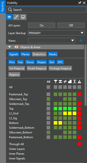
Step 16: The Visibility panel opens. From here, you can define colors for each element of the board. Choose the Layers mode.
Step 17: Right-click the color box under All for L2_Gnd.
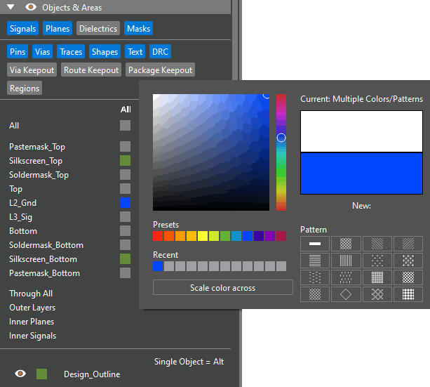
Step 18: A color selection dialog opens. Select Blue from the Presets and click outside the box to set the color.
Step 19: Right-click the color box under All for L3_Sig. Select Purple from the presets and click outside the box to set the color.
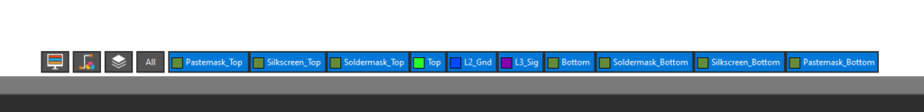
Step 20: View the floating layer toolbar. The layer colors are shown as assigned.
Wrap Up & Next Steps
Quickly add layers to a PCB stackup to create and communicate the vertical design intent of your board with the Cross-Section Editor in OrCAD X Presto. Test out this feature and more with a free trial of OrCAD. For more how-tos and step-by-step walk-throughs, visit EMA Academy.

