When routing differential pairs through a copper plane or pour, voiding is dependent on the defined spacing constraint; however, in some situations, impedance may need to be improved by configuring the via voiding as a pair or group instead of individually. With the high-speed option in Allegro PCB Designer, users can easily define the desired return path configuration and control the voiding to improve the differential pair impedance.
This quick how-to will provide step-by-step instructions on how to adjust the voiding for differential pair return path vias with the High-Speed Option in Allegro PCB Designer.
How-To Video
Configuring Via Voiding
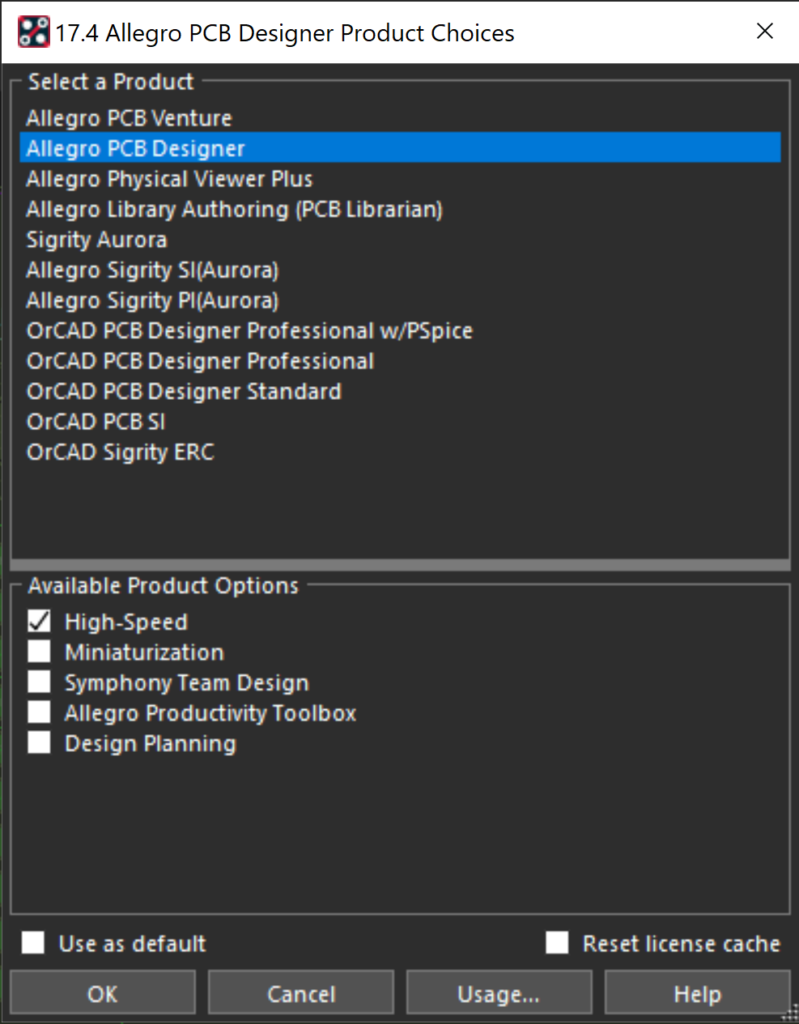
Step 1: Open the desired design in Allegro PCB Designer with the High-Speed Option enabled.
Step 2: Select Shape > Global Dynamic Params… from the menu.
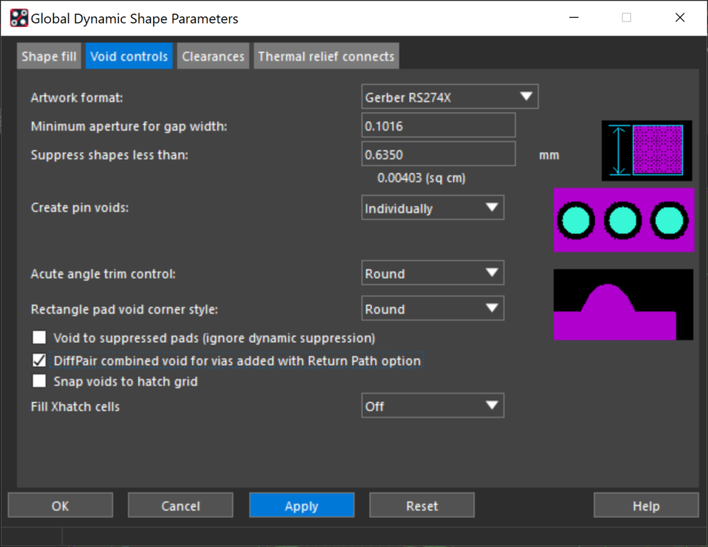
Step 3: Select the Void Controls tab and choose DiffPair combined void for vias added with Return Path option.
Step 4: Click Apply and OK.
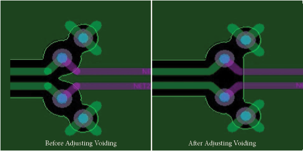
Note: The voided shape for the trace with return path vias added has been adjusted.
Adding Return Path Vias During Routing
Step 5: Select Route > Connect from the menu or the Add Connect button on the toolbar.
Step 6: Click to select one of the nets in the differential pair.
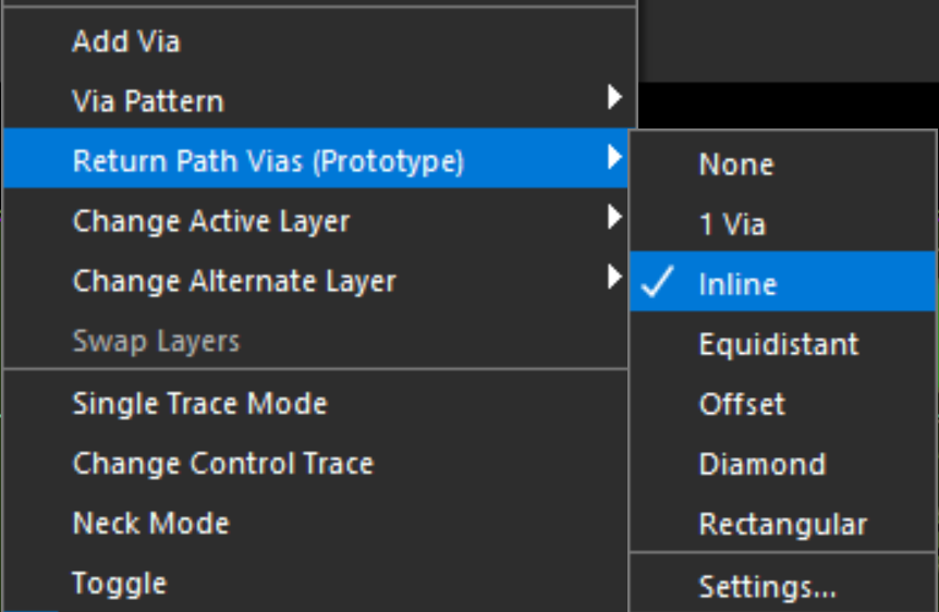
Step 7: Right-click and select Return Path Vias > In Line.
Note: Other Return Path Via Configurations are available including:
- 1 via: This pattern adds 1 return path via next to one of the differential pair vias.
- In Line: This pattern adds 2 return path vias aligned in a straight line with the differential pair vias.
- Equidistant: This pattern adds 1 return path via placed equidistant between the differential pair vias.
- Offset: This pattern adds 2 return path vias offset with respect to the differential pair vias.
- Diamond: This pattern adds 2 return path vias placed equidistant on each side of the differential pair vias.
- Rectangular: This pattern adds 4 return path vias in a rectangular/square pattern centered on the differential pair vias.
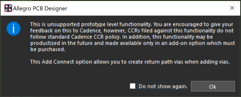
Step 8: If you receive a message that Return Path Vias is a prototype feature, click OK.
Note: If a return path via has not been configured, you will be prompted to set one up. Learn how to configure return path vias with this how-to.
Step 9: Double-click the PCB canvas to activate the via and return path configuration.
Note: The vias defined for the differential pair have been added to the cursor along with the selected return path vias.
Step 10. Click to place the vias on the PCB.
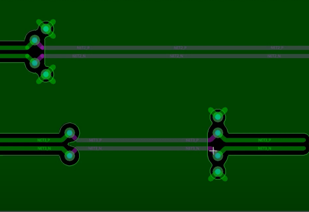
Step 11: Right-click and select Done. The clearance around the vias is grouped together rather than individually voided.
Wrap Up & Next Steps
Improve the impedance on high-speed differential pairs by controlling the return path via voiding when routing through copper with the high-speed functionality of Allegro PCB Designer. Check out our e-book to learn more about solving common issues for high-speed designs.

