
Step 2: Select the constraint manager icon from the constraints panel or select Electrical Analysis > Constraint Manager from the menu.
Step 3: Select Manufacturing Worksheet. Expand Design for Assembly > DFA Constraint Set and select PkgToPkg Spacing.
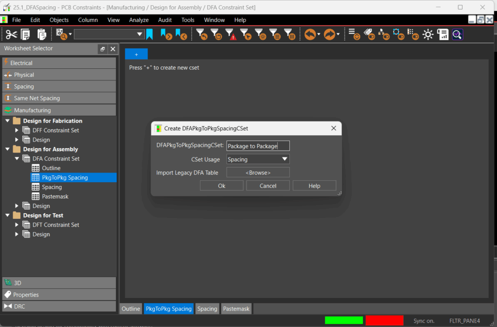
Step 4: Select the + sign to create a new package to package spacing constraint set. A constraint set can contain multiple rules for easy assignment and reuse.
Step 5: Name the constraint set Package to Package and click OK.
Step 6: The constraint set window is opened containing a graphic displaying the constraints which will be configured including package to package spacing based on the component rotation and orientation on the board: side to side, end to end, side to end, and end to side. Select Show Symbol Classifications.
Step 7: View the symbol classifications. The DFA_DEV_CLASS property has been defined so these are automatically populated in the DFA package to package constraint window. Click OK.
Step 8: The DFA package to package spacing window now shows a matrix feature the relationships between symbol classifications. All spacing fields have the default value of 25 mils.
Define DFA Package to Package Spacing Values
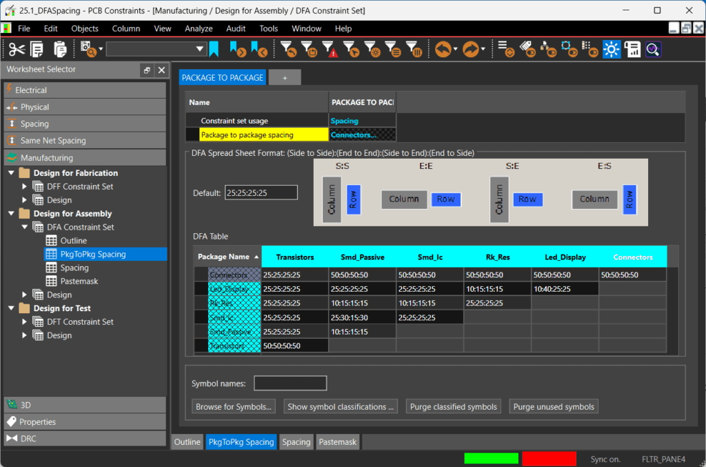
Step 9: Click and drag to highlight the values in the connector row. Upon release of the mouse, the last column is activated to edit the text. Change the values to 50:50:50:50 and press Enter. This will ensure the spacing between connectors and any other components in any orientation is 50 mils.
Step 10: Select the cell to define the relationship between LED_Display and Rk_Res. Change the values to 10:15:15:15 and press Enter. This will define the proper spacing requirements between the LED Display and resistors.
Step 11: Select the cell to define the relationship between LED_Display and LED_Display. Change the values to 10:40:25:25 and press Enter. This will define the proper spacing requirements between components in the LED Display.
Step 12: Click and drag to highlight the values in the Rk_Res for SMD_Ic and SMD_passive. Change the values to 10:15:15:15 and press Enter.
Step 13: Select the cell to define the relationship between SMD_lc and SMD_Passive. Change the values to 25:30:15:30 and press Enter.
Step 14: Select the cell to define the relationship between SMD_Passive and SMD_Passive. Change the values to 10:15:15:15 and press Enter.
Step 15: Select the cell to define the relationship between Transistors. Change the values to 50:50:50:50 and press Enter.
Assign DFA Spacing Constraints
Step 16: In the Design for Assembly section, expand Design. Select PkgtoPkg Spacing.
Step 17: Expand Primary and Assembly Layers.
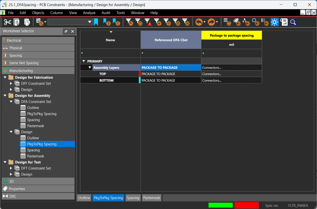
Step 18: Click the Referenced DFA CSet cell for the Assembly Layers and select Package to Package. The defined package to package spacing values have been assigned to both the Top and Bottom assembly layers.
Activate DFA Constraint Checks in OrCAD X
Step 19: In order to check if the design meets the DFA spacing requirements defined, the constraint checks need to be enabled. Select Analyze > Analysis Modes from the menu.
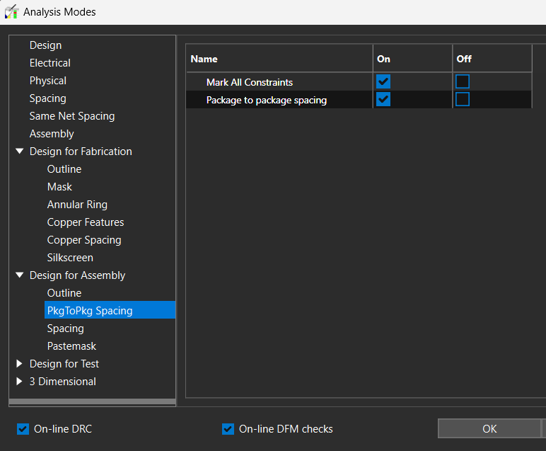
Step 20: Expand the Design for Assembly section and select PkgToPkg Spacing.
Step 21: Select the checkbox for On. Click OK.
Step 22: Close the constraint manager window.
Verify DFA Constraint Adherence
Step 23: Select the Properties tab and view the DRC Chart. There are 7 Design for Assembly violations.
Step 24: Select the hyperlink for the DRC Errors to open more information in the Search panel.
Step 25: Double click a DFA violation in the search panel to be brought to the location on the PCB. For the example we will select the violation between R6 and R3 on the bottom of the PCB.
Step 26: A DRC marker flags the error and additional information can be viewed by hovering the cursor over the marker. Here the Side to Side spacing should be 10 mils but it is only 5 mils.
Correct DFA Issues During PCB Layout
Step 27: In the Selection Filter. Select All Objects to turn all objects off, then select Components.
Step 28: Select the Move icon from the toolbar.
Step 29: In the Options panel, select Relative Grid. This will allow you to move components based on a defined origin and enable us to easily move the resistor the additional 5 mils away.
Step 30: Select Pick Relative Origin. Click to select the bottom corner of component R6.
Step 31: Select the bottom corner of R6 again to move the component. Press TAB on the keyboard to be able to edit the DX and DY values.
Step 32: Enter 5 for DX. Press Tab on the keyboard. Enter 0 for DY, then press Enter.
Step 33: The component has been moved the required distance away and the DRC marker is removed. The remaining DFA errors can be corrected in the same manner to ensure manufacturability and assembly.
Step 2: Select the constraint manager icon from menu or Setup > Constraints from the menu.
Step 3: Select Manufacturing Worksheet. Expand Design for Assembly > DFA Constraint Set and select PkgToPkg Spacing.
Step 4: Select the + sign to create a new package to package spacing constraint set. A constraint set can contain multiple rules for easy assignment and reuse.
Step 5: Name the constraint set Package to Package and click OK.
Step 6: The constraint set window is opened containing a graphic displaying the constraints which will be configured including package to package spacing based on the component rotation and orientation on the board: side to side, end to end, side to end, and end to side. Select Show Symbol Classifications.
Step 7: View the symbol classifications. The DFA_DEV_CLASS property has been defined so these are automatically populated in the DFA package to package constraint window. Click OK.
Step 8: The DFA package to package spacing window now shows a matrix feature the relationships between symbol classifications. All spacing fields have the default value of 25 mils.
Define DFA Package to Package Spacing Values
Step 9: Click and drag to highlight the values in the connector row. Upon release of the mouse, the last column is activated to edit the text. Change the values to 50:50:50:50 and press Enter. This will ensure the spacing between connectors and any other components in any orientation is 50 mils.
Step 10: Select the cell to define the relationship between LED_Display and Rk_Res. Change the values to 10:15:15:15 and press Enter. This will define the proper spacing requirements between the LED Display and resistors.
Step 11: Select the cell to define the relationship between LED_Display and LED_Display. Change the values to 10:40:25:25 and press Enter. This will define the proper spacing requirements between components in the LED Display.
Step 12: Click and drag to highlight the values in the Rk_Res for SMD_Ic and SMD_passive. Change the values to 10:15:15:15 and press Enter.
Step 13: Select the cell to define the relationship between SMD_lc and SMD_Passive. Change the values to 25:30:15:30 and press Enter.
Step 14: Select the cell to define the relationship between SMD_Passive and SMD_Passive. Change the values to 10:15:15:15 and press Enter.
Step 15: Select the cell to define the relationship between Transistors. Change the values to 50:50:50:50 and press Enter.
Assign DFA Spacing Constraints
Step 16: In the Design for Assembly section, expand Design. Select PkgtoPkg Spacing.
Step 17: Expand Primary and Assembly Layers.
Step 18: Click the Referenced DFA CSet cell for the Assembly Layers and select Package to Package. The defined package to package spacing values have been assigned to both the Top and Bottom assembly layers.
Activate DFA Constraint Checks in OrCAD X
Step 19: In order to check if the design meets the DFA spacing requirements defined, the constraint checks need to be enabled. Select Analyze > Analysis Modes from the menu.
Step 20: Expand the Design for Assembly section and select PkgToPkg Spacing.
Step 21: Select the checkbox for On. Click OK.
Step 22: Close the constraint manager window.
Verify DFA Constraint Adherence
Step 23: Select the DRC tab in the search panel. There are 7 DRC Errors.

