When importing PCB features, such as board outlines and RF elements, the source file may be written as a series of lines rather than closed geometry. In these situations, the imported lines and arcs must be closed or converted to a shape so that they can be handled as one object rather than individual elements. In OrCAD X, the Create Shape from Lines tool can be used to quickly and easily generate a shape, ensuring the correct representation for design elements and improve the PCB layout process.
This quick how-to will provide step-by-step instructions on how to create a shape from lines in OrCAD X.
To follow along, download the provided files above the table of contents.
How-To Video
 Open in New Window
Viewing Lines on the Canvas
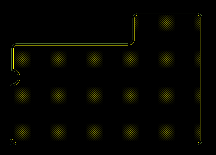
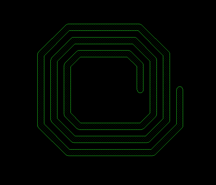
Step 1: Open the provided design, Line_Outline.brd in OrCAD X.
Step 2: Hover over one of the lines that makes up the board outline. Only the selected line is highlighted.
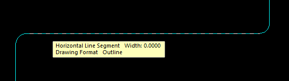
Step 3: View the tooltip. Each drawn line is in the Drawing Format/Outline class/subclass.
Create a Shape from Lines: Board Outline
Step 4: To create a shape from lines, select Shape > Create Shape from Lines from the menu.
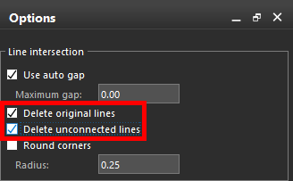
Step 5: In the Options panel, check Delete Original Lines and Delete Unconnected Lines.
Step 6: Set the Active Class and Subclass to the desired selection. For this example, select Board Geometry and Design Outline.
Step 7: Uncheck the option for Filled Shape.
Note: This option can be checked if creating a copper plane or pour in the design.

Step 8: Click and drag to select the board outline in the canvas. The line color changes to green, indicating that the figure has changed layers. Right-click and select Done.
Step 9: Hover your cursor over the shape again. The entire shape is now highlighted and the tooltip indicates that the shape is now in the Board Geometry/Design Outline class and subclass.
Create a Shape from Lines: Filled Shape
Step 10: A filled shape can also be created from lines. We will create a plane on the board to demonstrate. The lines for this plane have already been drawn but are not visible. To adjust visibility, select the Color button from the toolbar.
Step 11: In the Color Dialog window, select Drawing Format from the list on the left to open the Drawing Format table.
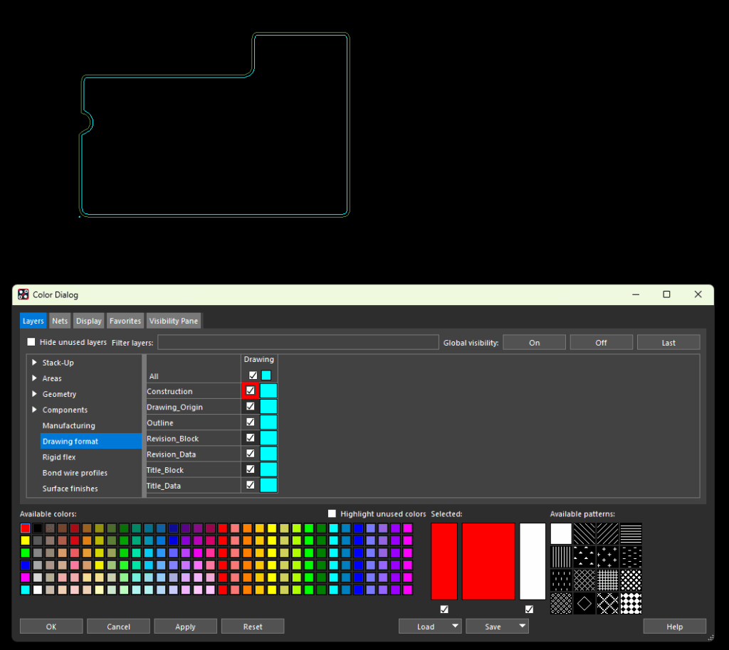
Step 12: Check the option for Construction to enable visibility for the Construction layer. The hidden layer is visible on the PCB canvas. Click OK in the Color Dialog window to save the settings and close the window.
Step 13: Select Shape > Create Shape from Lines from the menu.
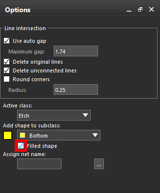
Step 14: In the Options panel, select Etch and Bottom for the Active Class and Subclass. Check Filled Shape to create a filled shape.
Note: In a board with a full netlist, the net the shape is assigned to can also be configured here.
Step 15: Click each segment of the new shape. When all segments are selected, the shape changes color and is filled, indicating that the lines and arcs were converted into a solid shape. Right-click and select Done.
Creating a Dynamic Shape
Step 16: The created shape is static. To create a dynamic shape with healing properties, select Setup > Application Mode > Shape Edit from the menu.
Note: Alternatively, right-click and select Application Mode > Shape Edit, or select Shape Edit from the Application Mode list in the bottom-right corner of the window.
Step 17: Right-click the newly-created shape and select Change Shape Type to Dynamic.
Step 18: A prompt appears that this conversion will result in the loss of the original shape boundary. Click Yes to proceed.

Step 19: View the canvas. The shape is now completely solid, indicating that it is dynamic. If a net is assigned, the shape will “heal” to any other copper nets running through it and automatically trim parts outside the design outline.
Step 20: Select Setup > Application Mode > General Edit to return to the General Edit mode.
Create a Shape from Lines: RF Elements
Step 21: For high-frequency boards, elements such as RF planes and in-board inductors can be imported from DXF files as lines and converted to shapes. For better visibility, in the Visibility panel, select Etch for Bottom to disable the visibility of the newly-created bottom etch.
Step 22: Select Import > MCAD > DXF from the menu.
Step 23: The DXF In window opens. Here you can configure the file to load, the units, accuracy, and layer mapping. Select the ellipsis for DXF File to select the file.
Step 24: Select the provided RF.dxf file and click Open.
Step 25: A layer mapping file must be defined to import the drawing file. Under Conversion Profile, select Edit/View Layers.
Step 26: The DXF In Edit/View Layers window opens, showing a table of DXF layers and how they are to be mapped. Check Select for the sole layer listed.
Step 27: Under Map Selected Items, select Drawing Format from the Class dropdown and Construction from the Subclass dropdown.
Step 28: Select Map. The layers are mapped. Click OK.
Step 29: Check Incremental Addition to add the DXF to the current board.
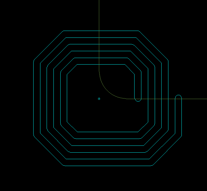
Step 30: Select Import. The RF coil is imported as lines. Click Close in the DXF In window.
Step 31: Uncheck Shape in the Find panel. Click and drag to select the lines to move them.
Step 32: Select the Move mode from the toolbar. Click the lines to select them and attach them to your cursor. Move the lines into the board outline and click to place. Right-click and select Done.
Step 33: Select Shape > Create Shape from Lines from the menu.
Step 34: In the Options panel, set the active class and subclass to Etch and Top. Check Filled Shape, Delete Original Lines, and Delete Unconnected Lines.
Step 35: Click and drag in the canvas to select the imported RF lines. The lines turn green and are filled, indicating that they have been converted to a static shape. Right-click and select Done.
Wrap Up & Next Steps
Quickly and easily create a shape from lines in OrCAD X to complete your PCB layout efficiently. Test out this feature and more with a free trial of OrCAD X. Get more how-tos for OrCAD X at EMA Academy.

