Nearly every component in a circuit requires a connection to power and ground. To ensure a robust connection, power and ground planes are used to make power and ground available throughout the board. However, especially with modern designs, plane creation can be complicated due to:
- Multiple voltage nets required
- Multiple ground nets required
- Limited number of planes due to manufacturing requirements
These requirements can increase board thickness, add to manufacturing costs, and make PCB layout more complex. With OrCAD X, easily create a split plane to accommodate multiple voltage nets on the same layer, reducing cost and saving layer space.
To follow along, download the provided files above the table of contents.
How-To Video
 Open in New Window
Creating a Layer Plane
Step 1: Open the provided design in OrCAD X PCB Designer.
Step 2: The split plane tool can also be used to generate a full plane on a layer and divide it after placement. To do this, select Edit > Split Plane from the menu.
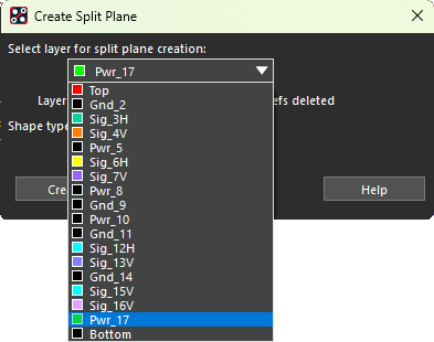
Step 3: The Create Split Plane window opens. Choose PWR_17 from the layer dropdown.
Step 4: Click Create to create the plane.
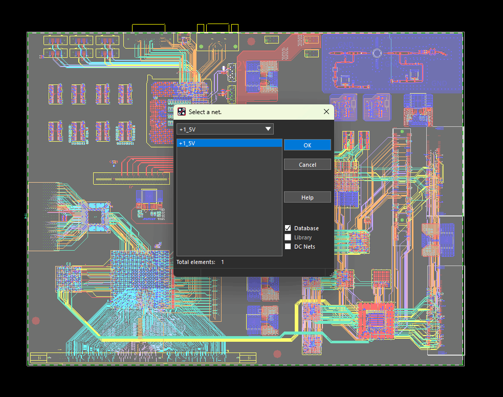
Step 5: The net assignment window opens. Select +1_5V from the list to assign the 1.5V net to the new plane and click OK.
Create a Split Plane in OrCAD X
Step 6: To define where the plane is split a Split Line must be created. To create a split line, select Add > Line from the menu.
Step 7: In the Options panel, set the active class to Anti Etch and the active subclass to PWR_17.
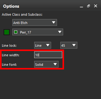
Step 8: Set the line width to 10 mils and the line font to Solid. This will create a 10 mil gap between the split planes.
Step 9: To ensure a thorough cut, start drawing a line outside of the board outline cut the plane in half. Click the other side of the board, outside of the board outline, to finish. When finished, right-click and select Done.
Step 10: To finalize the plane split, select Edit > Split Plane from the menu again.
Step 11: Select layer PWR_17 from the dropdown and click Create.
Note: If prompted that the split may lead to DRC violations, click Yes to proceed.
Step 12: The Select a Net window opens for the first plane, which is highlighted on the canvas. +1_5V is already selected- leave the selection and click OK.
Step 13: The second plane becomes visible on the canvas. Check DC Nets in the Select a Net window.
Step 14: Select * from the dropdown to view all available DC nets.
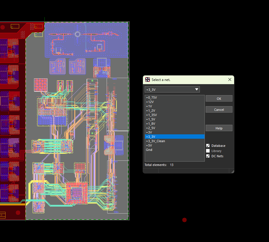
Step 15: Select +3_3V from the list to assign the 3.3V net to the right-side plane. Click OK.
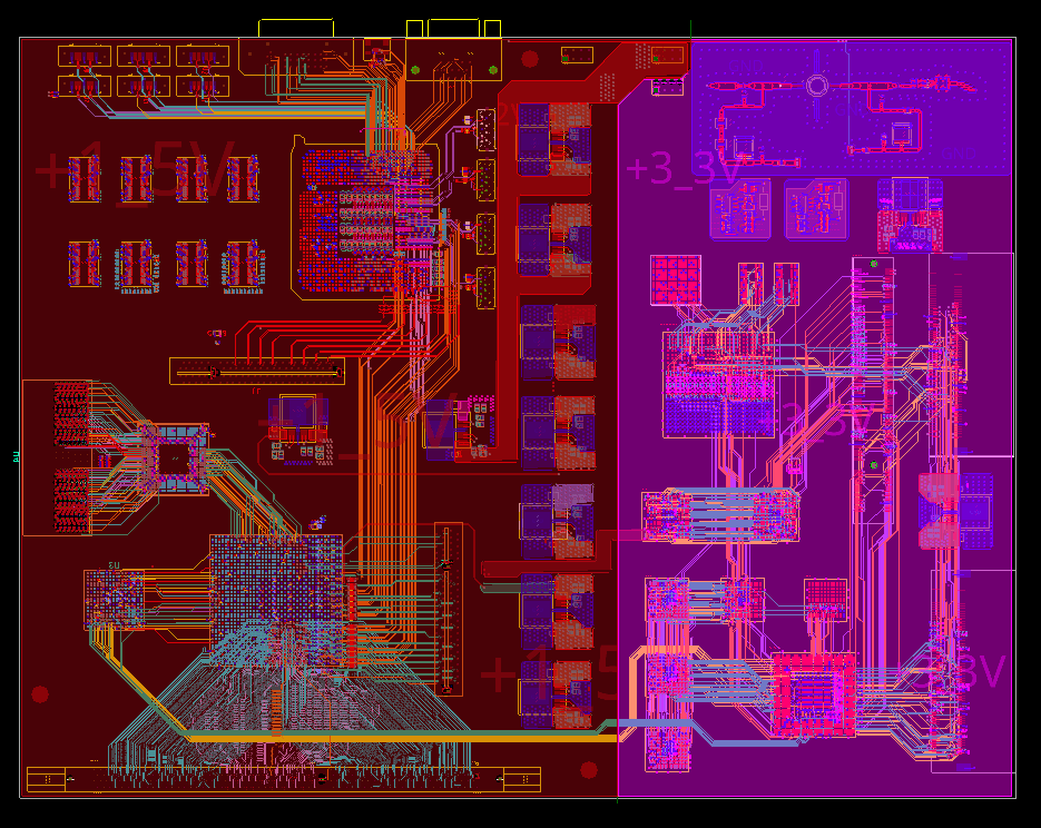
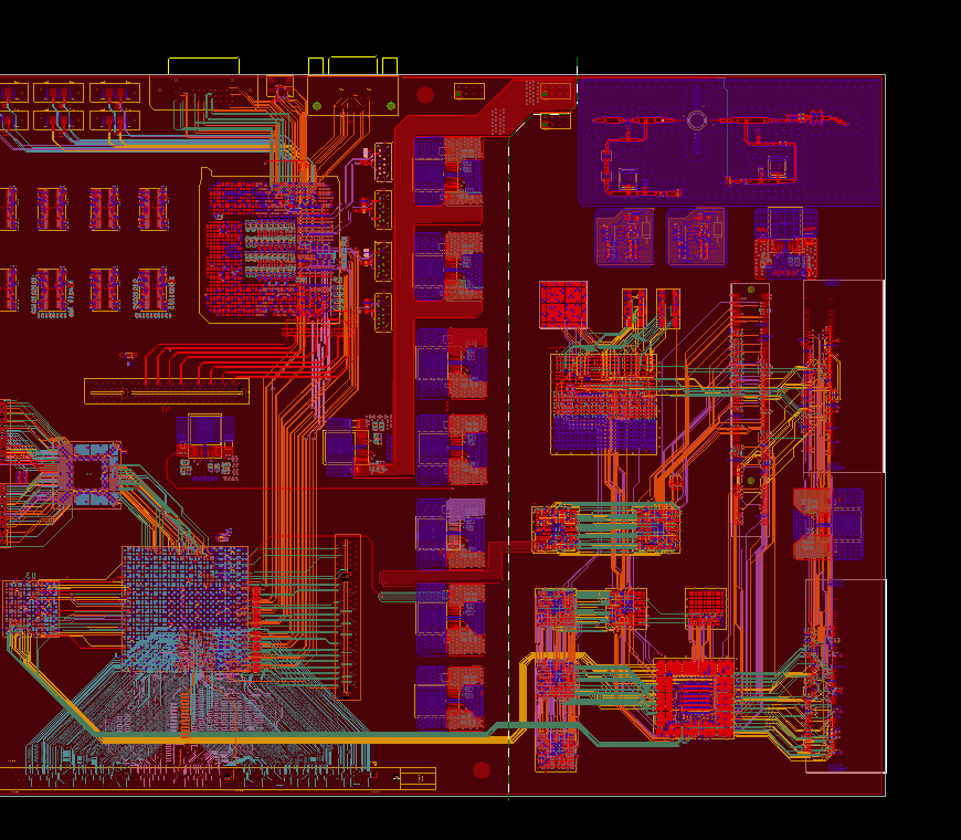
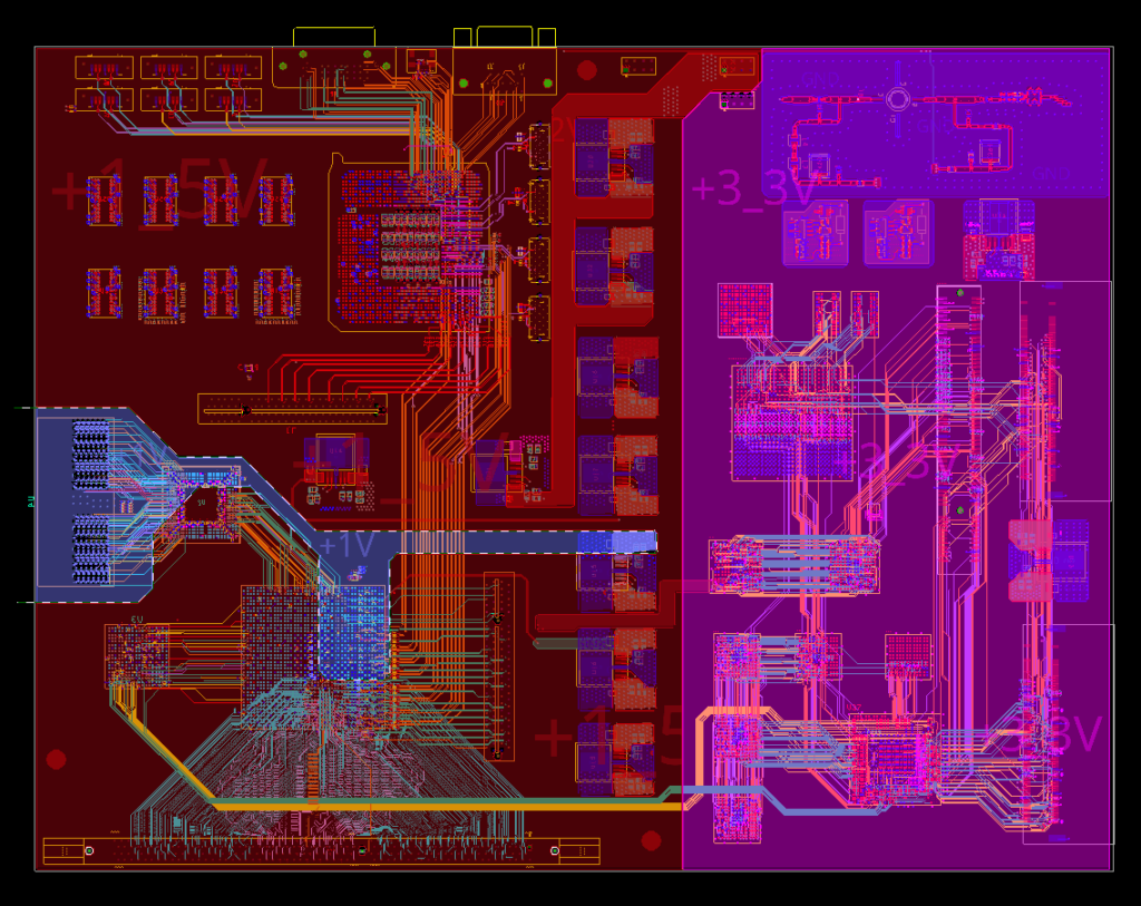
Step 16: View the PCB canvas. The left plane is assigned to 1.5V and the right plane to 3.3V.
Create an Enclosed Split Plane in OrCAD X
Step 17: Planes can also be split such that they are surrounded by another net. To do this, select Add > Line from the menu.
Step 18: In the Options panel, set the active class to Anti Etch and subclass to PWR_17. Set the line width to 10 mils.
Step 19: Click to start drawing a polyline around the desired split plane. Start and end the line outside the shape. When finished, right-click and select Done.
Step 20: Select Edit > Split Plane from the menu.
Step 21: Select layer PWR_17 from the dropdown and click Create.
Note: If prompted that the split may lead to DRC violations, click Yes to proceed.
Step 22: The new plane is highlighted for net selection. Check DC Nets and select * from the dropdown.
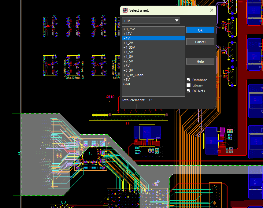
Step 23: Select +1V from the list to assign the 1V net to the new plane. Click OK.
Step 24: The other planes are highlighted with their previous net assignments automatically selected. Click OK for both planes.
Remove the Anti-Etch Lines
Step 25: To remove the anti-etch lines used to generate the split plane, select the Delete mode from the toolbar.
Step 26: Check Lines in the Find panel to allow the lines to be selected.
Step 27: Click the previously-drawn anti-etch lines to remove them and clean up the board. When finished, right-click and select Done.
Wrap Up & Next Steps
Quickly and easily create a split plane to limit the number of layers required for your design and ensure a robust connection to power and ground with the split plane feature in OrCAD X. Test out this feature and more with a free trial of OrCAD X. Get more how-tos for OrCAD X at EMA Academy.

