
Create Keepins from the Properties Panel
Step 1: Open the provided design in OrCAD X Presto.
Step 2: Route keepins can be used to ensure traces, vias, and other conductive objects stay within a defined boundary. By default, a route and conductor keepin are attached to a new design outline in OrCAD X Presto. Click to select the outline.
Step 3: In the Properties panel, check the option for Conductor Keep-In. A conductor keepin is added to the outline.
Step 4: Enter 0.8 for the Conductor Keep-in amount to contract the keepin by 0.8mm.
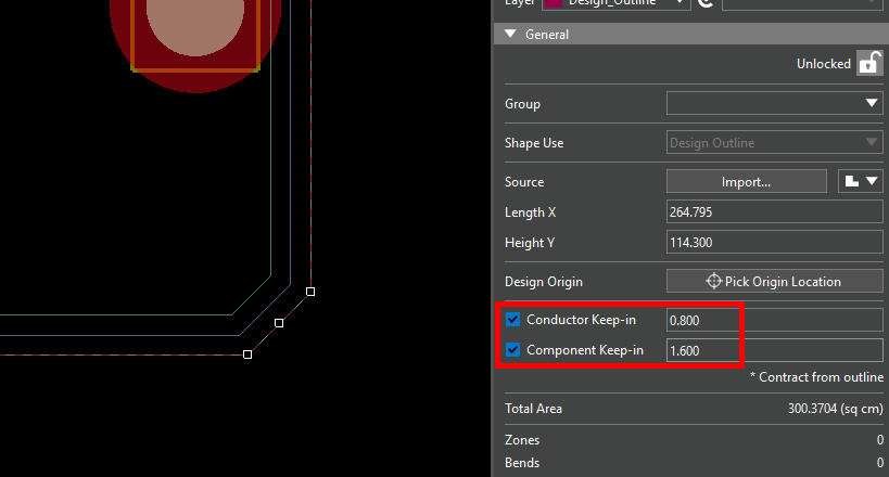
Step 5: Check the option for Component Keep-In and enter 1.6 for the amount to contract the keepin by 1.6mm. The keepins are added to the design outline.
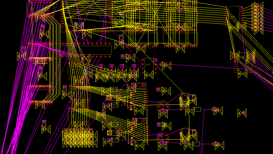
Step 6: Pan the view to the unplaced components at the top of the board. All are indicated with DRC markers, as they are now outside the keepin zone.
Creating a Route Keepout
Step 7: Route keepouts can be used to prevent traces, vias, and other conductor objects from being placed in a defined area. To create a route keepout shape, right-click Shape Utilities in the toolbar and select Add Shape.
Step 8: Select Rectangle in the Add Shape widget to draw a rectangle.
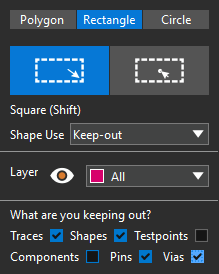
Step 9: Select Keep-Out for the shape use and All for the layer.
Step 10: Check the options to keep out Traces, Shapes, Pins, and Vias to keep out all conductors.
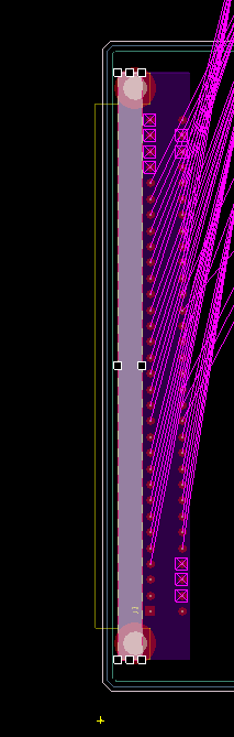
Step 11: Click to start drawing the rectangle in the keepout zone shown above and click again to finish.
Step 12: Choose the Select mode from the toolbar to end the shape drawing mode.
Step 13: To test the keepout, select the Add Connect mode from the toolbar.
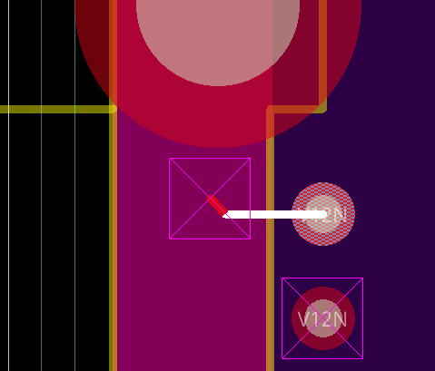
Step 14: Click to start drawing a trace on one of the nearby pins. When your cursor enters the keepout zone, the attached trace turns white, indicating that placing the trace will create a DRC error.
Choose the Select mode to end trace placement.
Creating a Package Keepout
Step 15: Package keepouts can be used to prevent component placement within a defined area. To create a package keepout, select the Add Shape mode from the toolbar.
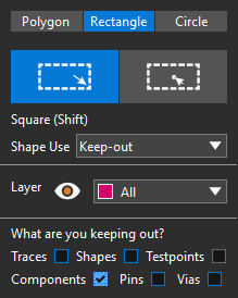
Step 16: In the Add Shape widget, set the Shape Use to Keep-out, the Layer to All, and check Components. Uncheck all other exclusions.
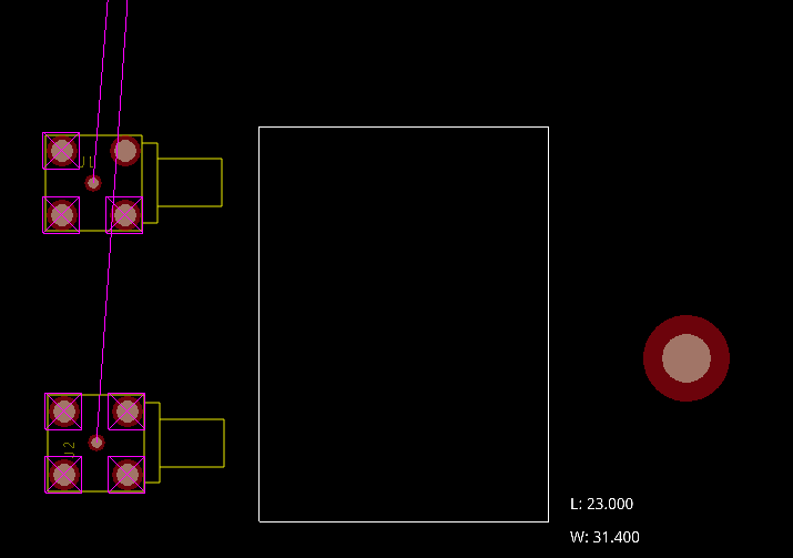
Step 17: Click to start drawing the rectangle in front of the BNC connectors and click again to finish.
Step 18: To test the keepout, select the Move mode from the toolbar.
Step 19: Select a component from the top edge of the board to attach it to your cursor.
Step 20: Click to place the component in the keepout zone.
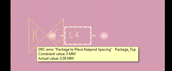
Step 21: A DRC error is created. Choose the Select mode from the toolbar and hover over the violation to view a tooltip for more information. The tooltip indicates that the package violates the keepout.
Creating a Route Keepin
Step 1: Open the provided design in OrCAD X PCB Designer.
Step 2: Route keepins can be used to ensure traces, vias, and other conductive objects stay within a defined boundary. To create a route keepin in PCB Designer, the Z-Copy feature can be used to match the board outline. Select Shape > Z-Copy from the menu.
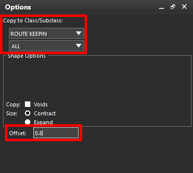
Step 3: In the Options panel, set the target class and subclass to Route Keepin and All.
Step 4: Select Contract under Size. Enter 0.8 for the offset to contract the shape by 0.8mm.
Step 5: Select the board outline to create the contracted copy.
Creating a Package Keepin
Step 6: Package/component keepins can be used to ensure components and packages stay within a defined boundary on the PCB.
In the Options window for Z-Copy, set the active class and subclass to Package Keepin and All.
Step 7: Select the route keepin outline to create a further contracted copy. The package keepin is drawn. Right-click and select Done to end the Z-Copy command.
Step 8: Select the DRC button in the bottom-right corner of the canvas and click Update. The DRC cache is updated and several DRC markers are shown on the top edge of the board, indicating the (unplaced) components outside the package keepin.
Creating a Route Keepout
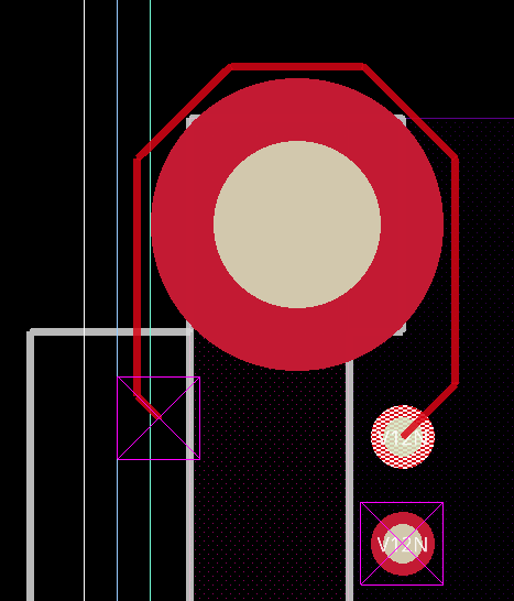
Step 9: Route keepouts can be used to prevent traces, vias, and other conductor objects from being placed in a defined area. To create a route keepout shape, select Shape > Rectangular from the menu.
Step 10: In the Options panel, set the active class and subclass to Route Keepout and All.
Step 11: Right-click the upper-left corner of the connector and select Snap Pick To > Segment Vertex to attach the keepout corner to the vertex.
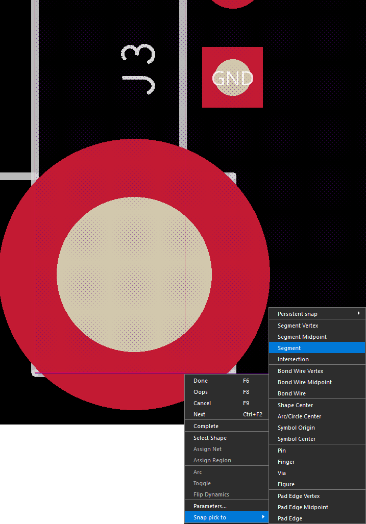
Step 12: Right-click the bottom edge and select Snap Pick To > Segment to place the keepout shape as shown.
Step 13: Right-click and select Done to end the drawing.
Step 14: To test the keepout, select Route > Connect from the menu.
Step 15: Click to start drawing a trace on one of the nearby pins. When your cursor enters the keepout zone, the attached trace reroutes to avoid the keepout area. If the attached trace turns white, a reroute was not possible and placing the trace will create a DRC error. Right-click and select Cancel to detach the trace.
Creating a Package Keepout
Step 16: Package keepouts can be used to prevent component placement within a defined area. To create a package keepout, select Shape > Rectangular from the menu.
Step 17: In the Options panel, set the active class and subclass to Package Keepout and All.
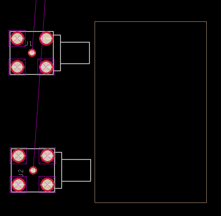
Step 18: Click to start drawing the shape in front of the BNC connectors and click again to finish. Right-click and select Done.
Step 19: To test the keepout, select the Move mode from the toolbar.
Step 20: Select one of the components on the top edge of the board to attach it to your cursor.
Step 21: Click to place the component inside the keepout zone. Right-click and select Done.
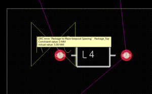
Step 22: A DRC marker appears. Hover over the violation to view a tooltip for more information. The tooltip indicates that the package violates the keepout.

