In many RF applications, shields are required for critical signals to minimize crosstalk and noise. Manually creating shields which follow the structure of the signal trace using dynamic or static shapes and connecting to ground can be a time-consuming process. Shield Routing in Allegro Productivity toolbox generates the desired shielding based on the inputted specifications to quickly shield RF signals and critical nets.
This how-to will provide step-by-step instructions on how to shield RF signal traces during routing and after traces are completed with Allegro Productivity Toolbox and OrCAD PCB Designer.
To follow along with this tutorial, use the provided designs above the table of contents.
How-To Video
Activating Shield Routing
Step 1: Open the provided design, demo.brd,in OrCAD PCB Designer Professional with the Allegro Productivity Toolbox option selected.
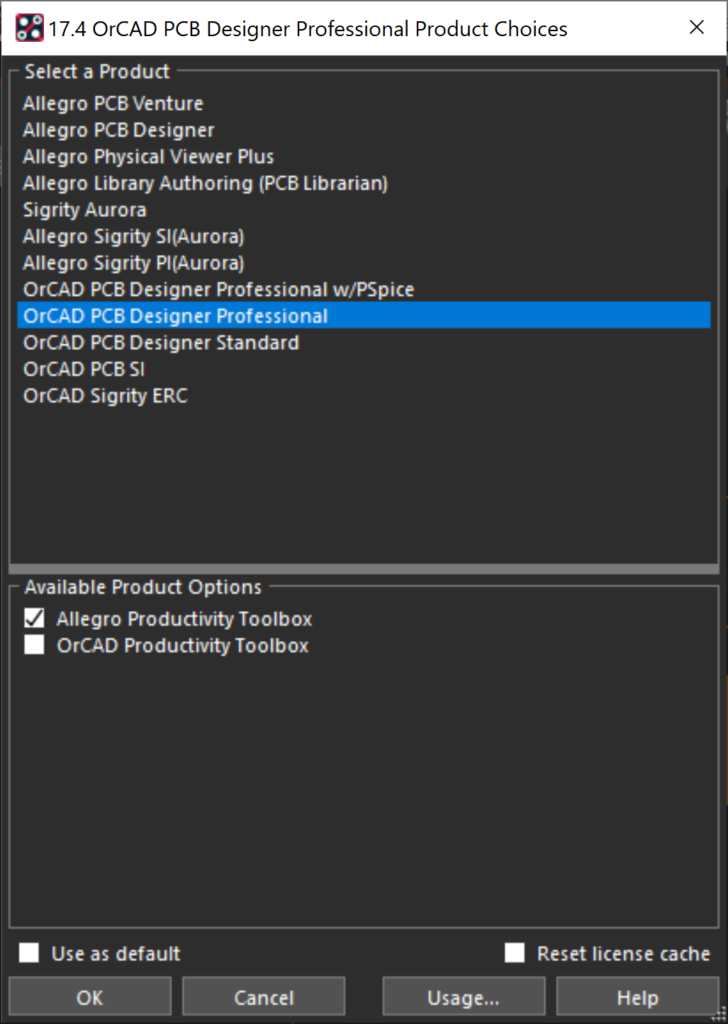
Note: Allegro Productivity Toolbox can be selected when launching OrCAD PCB Designer. To change licenses, select File > Change Editor.
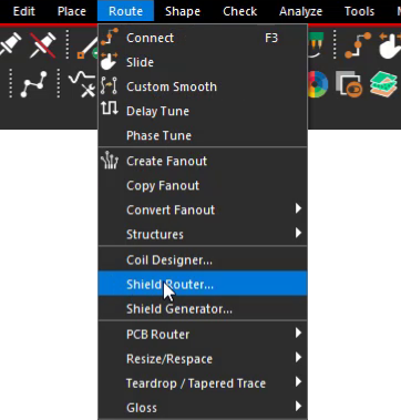
Step 2: Select Route > Shield Router from the menu.
Configuring Shield Routing Parameters
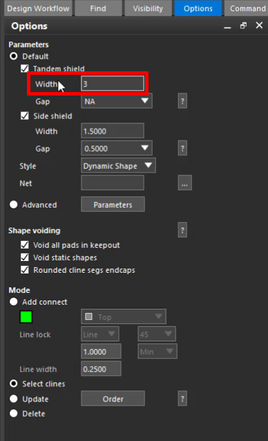
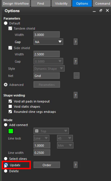
Step 3: In the Options tab, under Tandem Shield, set the Width to 3. Leave the default Gap value.
Note: A Tandem Shield will be added on layers above or below the trace.
- Width: Specifies the amount of oversizing.
- Gap: Specifies the size of the void inside the shielding. If the values is defined as NA, a gap or void will not be incorporated into the shield.
Step 4: Under Side Shield, set the Width to 2.5. Leave the default Gap value and Style.
Note: A Side Shield will be added on the same layer as the trace.
- Style: Select from Static Shape, Dynamic Shape, or Route Keepout.
Step 5: Select the ellipsis for the Net. The Select Net window will open.
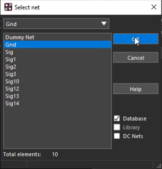
Step 6: Select Gnd from the net list and click OK.
Adding Shields While Routing
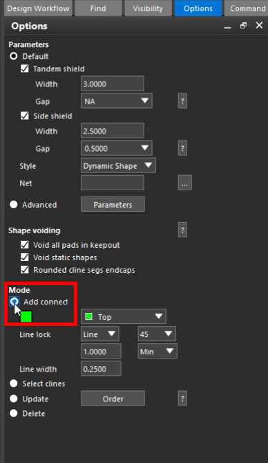
Step 7: In the Options tab, set the mode to Add Connect.
Note: In this mode, shields will be created while routing the signal trace. In this option, the following parameters can be defined:
- Line Width: Specify the width of the trace.
- Line Lock: Specify the type of trace as well as the preferred trace angle.
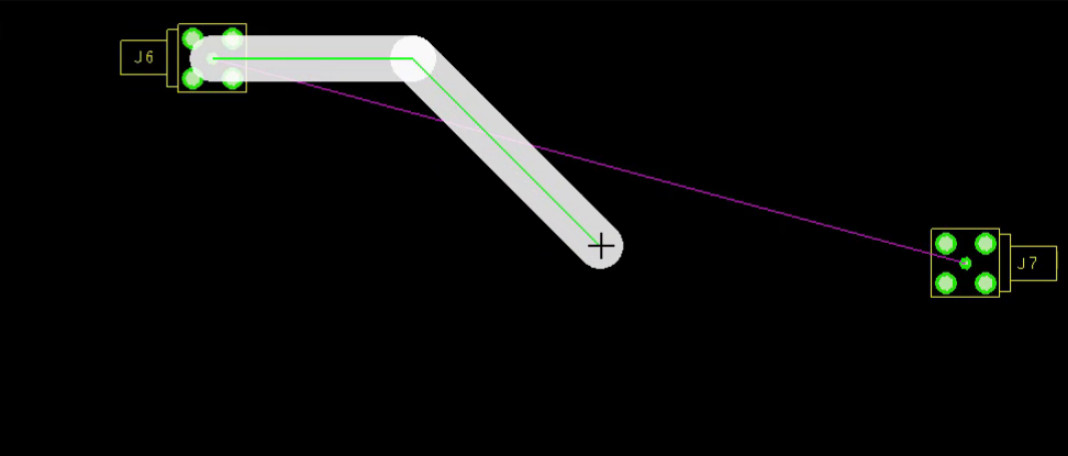
Step 8: Click in the center of connector J6 to begin routing a shielded trace. Click to place the trace.
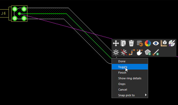
Step 9: About halfway through the routing, right-click and select Toggle.
Note: This reverses the locking sense of the next segment pair being added.
Step 10: Click to complete the routing.
Adding Shielding After Routing
Step 11: In the Options tab, set the mode to Select Clines.
Note: In this mode, the shield structure will be created by selecting existing traces.
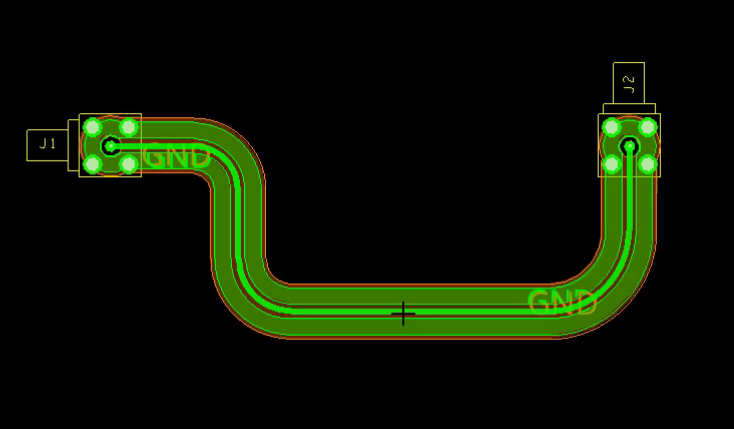
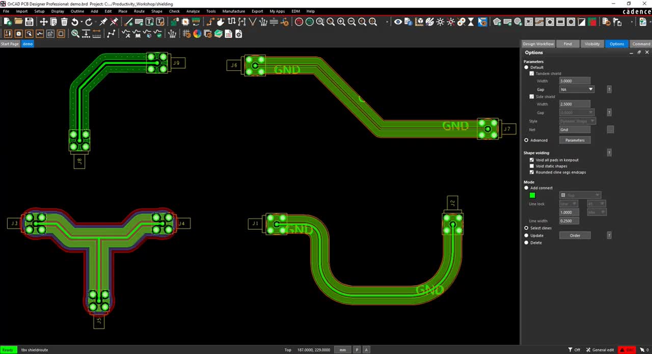
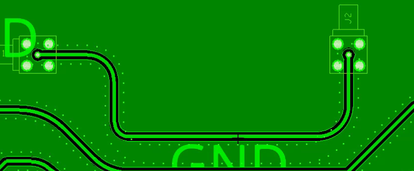
Step 12: Select the trace that connects J1 and J2. This will add shielding to the trace on its existing path.
Modifying Traces with Shields
Step 13: Select Route > Slide from the menu or the Slide button on the toolbar.
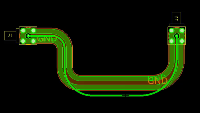
Step 14: Select a segment of the newly-shielded trace and slide it downwards. Click to place the trace.
Note: The shielding did not move with the trace and must be updated.
Step 15: Select Route > Shield Router from the menu.
Step 16: In the Options tab, ensure Select Clines is still selected as the mode. Click the trace to update the shielding.
Shielding on Multiple Layers
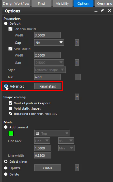
Step 17: Under Parameters, select Advanced.
Step 18: Select the Parameters button. The Shieldroute Advanced Settings window will open.
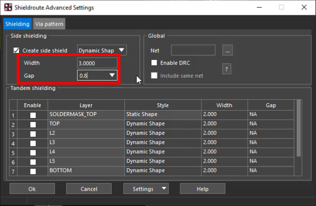
Step 19: Set the Width to 3 and the Gap to 0.8.
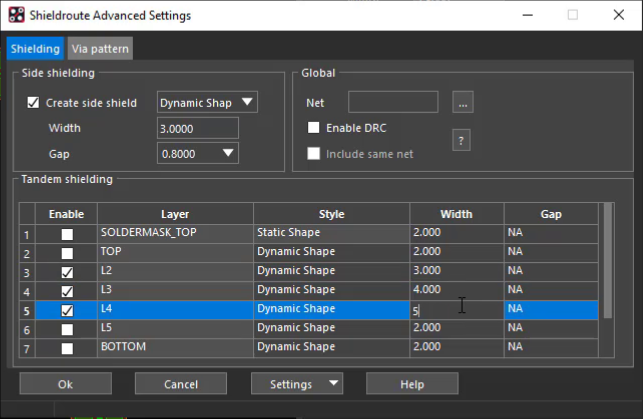
Step 20: In the Tandem Shielding table below, check the box under Enable for layers L2, L3, and L4.
Note: This will create the shield on multiple layers of the PCB.
Step 21: Still in the Tandem shielding table, set the following Widths:
- L2 to 3
- L3 to 4
- L4 to 5
Step 22: Click OK to save the settings and close the window.
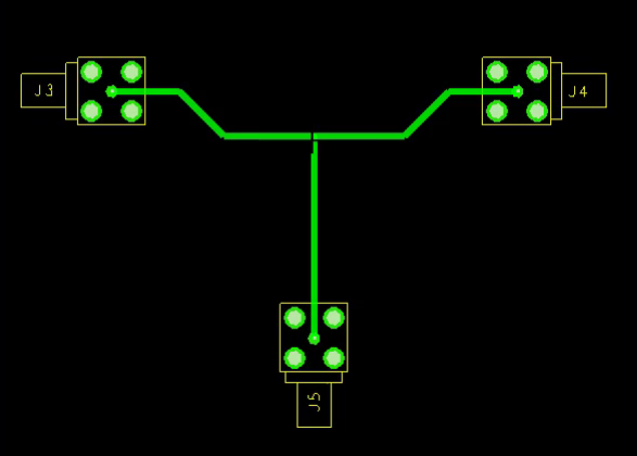
Step 23: Select one of the traces connecting J3, J4, and J5.
Step 24: A prompt will appear asking to confirm creation of the shield for a contiguous cline structure. Click Yes to create the shield.
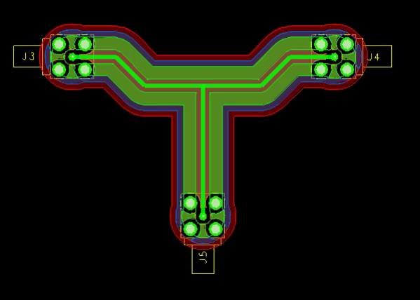
Note: The shield is created on layers L2, L3, and L4.
Incorporating Vias
Step 25: In the Options tab, under Advanced, select the Parameters button again.
Step 26: Select the Via Pattern tab at the top of the window.
Note: Some RF applications require additional shielding which can be accomplished by incorporating ground vias into the structure.
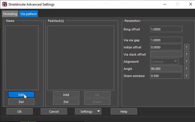
Step 27: Under Name table, select Add to add a new via pattern.
Step 28: Enter ring as the name and click OK.
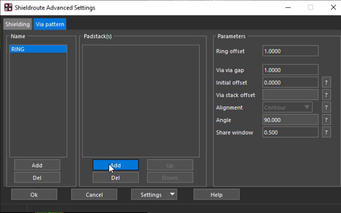
Step 29: Select RING from the Name table. Under the Padstacks table, select Add. The Select Via Padstack window opens.
Step 30: Type via* into the search bar and press Enter.
Note: This will search for padstacks that start with “via.”
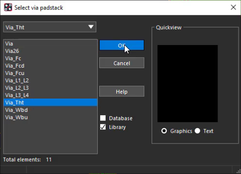
Step 31: Select padstack Via_Tht and click OK.
Step 32: Select the padstack Via_Tht from the Padstacks table.
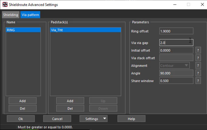
Step 33: Under Parameters, set the Ring Offset to 1.9.
Step 34: Set the Via via gap to 2.0. Leave all other values as the defaults and click OK.
Note: Additional parameters can be configured including:
- Initial Offset: Specifies the offset for the first via to be generated on the path. The default value is 0 which means the first via will be generated at the starting point of the path. This parameter is useful for tuning purposes when two or more rings need to be generated.
Step 35: Select the trace connecting J8 and J9.
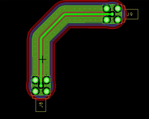
Note: This will create a shield across multiple layers with connecting vias.
Modifying Existing Shields
Step 36: In the Options tab under Advanced, select Parameters again.
Step 37: In the Tandem Shielding table, deselect the Enable option for L2, L3, and L4. Click OK.
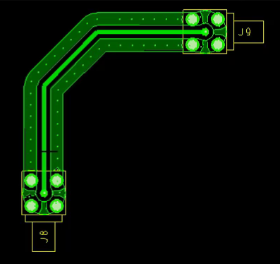
Step 38: Select the trace between J8 and J9 again.
Note: The shielding on all other layers has been removed.
Using a Pre-defined Via Pattern
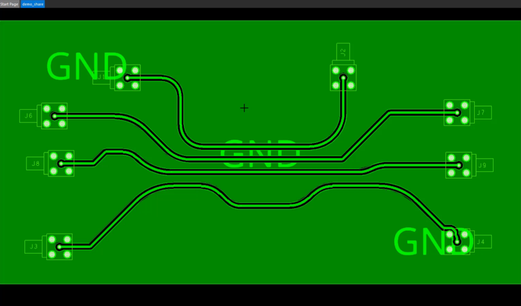
Step 39: Close the current demo.brd and open the provided design, demo_share.brd.
Step 40: Select Route > Shield Router from the menu.
Step 41: Select the ellipsis for the Net. The Select Net window will open.
Step 42: Select Gnd from the net list and click OK.
Step 43: In the Parameters section, select Advanced and select the Parameters button.
Step 44: Select the Via Pattern tab at the top of the window.
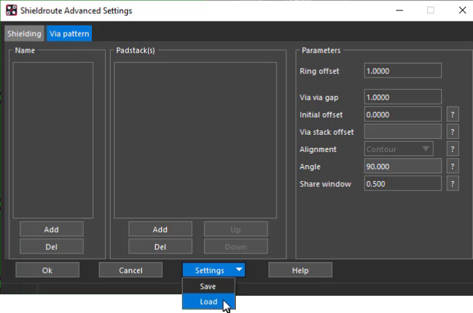
Step 45: Select Settings > Load.
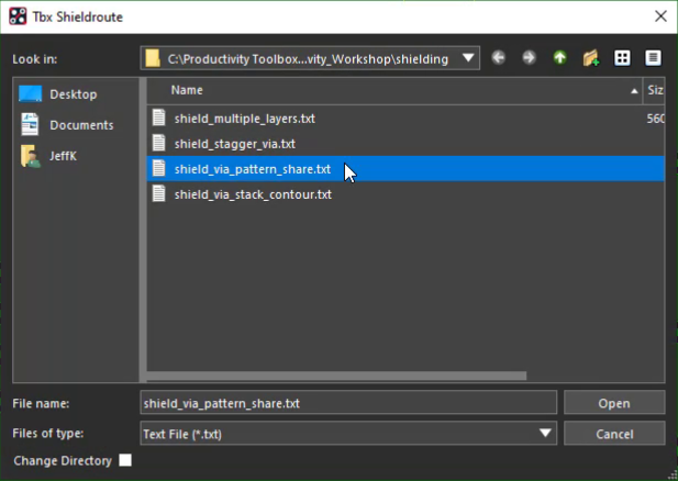
Step 46: Select the provided file, shield_via_pattern_share.txt, and click Open.
Step 47: Select the padstack Via_Tht from the Padstacks table. Leave the default values and click OK.
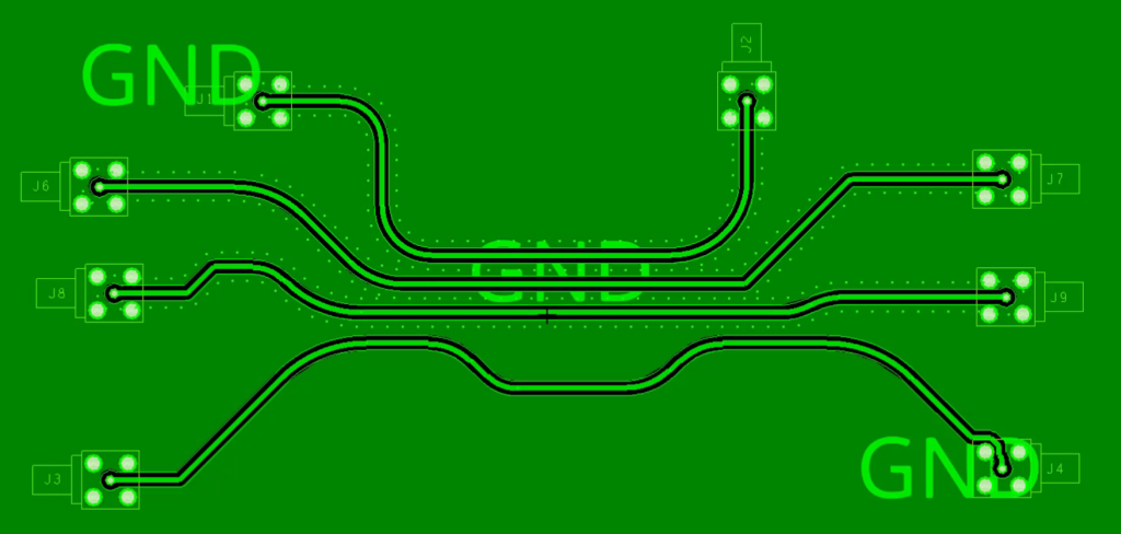
Step 48: Select the trace connecting J1 and J2.
Step 49: Select the trace connecting J6 and J7.
Step 50: Select the trace connecting J8 and J9.
Modifying a Shielded Trace
Step 51: Select Route > Slide from the menu or the Slide button from the toolbar.
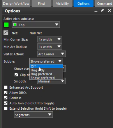
Step 52: In the Options tab, select the Bubble drop-down menu and choose Off.
Step 53: Select the trace connecting J1 and J2. Slide the trace upward and click to place.
Note: The surrounding dynamic copper pour heals itself but the shielding vias do not automatically update.
Updating Trace Shielding
Step 54: Select Route > Shield Router from the menu.
Step 55: In the options tab, set the mode to Update.
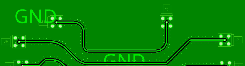
Step 56: Select the trace connecting J1 and J2.
Step 57: Select the trace connecting J6 and J7.
Note: The shielding vias have been updated.
Wrap Up & Next Steps
Proper shielding for critical nets in RF designs can be time-consuming when using manual methods for shape creation and via placement. Easily define shielding parameters and automatically generate shields and vias following the trace structure with the Shield Router in Allegro Productivity Toolbox. Learn more about the time-saving functionality included in Productivity Toolbox with our free webinar.

