In many RF and power applications, inductors need to be etched directly onto the PCB. Due to the tedious process of designing and laying out the trace in a spiral pattern, engineers often rely on external drafting tools to create a coil and import the final structure using DXF or Gerber; however, these methods are time-consuming and cumbersome. With Coil Designer in Allegro Productivity Toolbox, spiral inductors are automatically created based on the specified parameters for quick and efficient implementation without leaving the PCB canvas.
This how-to will provide step-by-step instructions on how to use Coil Designer to create a spiral inductor based on parameters and place the coil on the PCB.
How-To Video
Activating Coil Designer
Step 1: Open the desired design in OrCAD PCB Designer Professional with the Allegro Productivity Toolbox option selected.
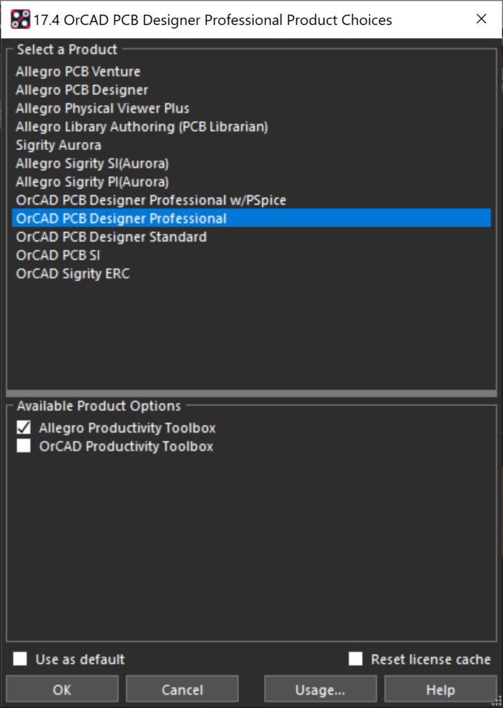
Note: Allegro Productivity Toolbox can be selected when launching OrCAD PCB Designer. To change licenses, select File > Change Editor.
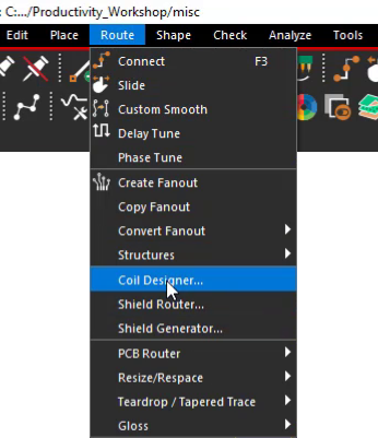
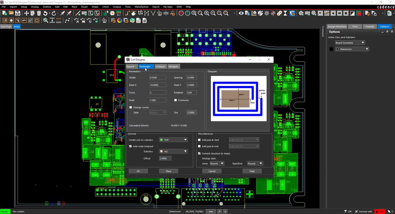
Step 2: Select Route > Coil Designer from the menu to open the Coil Designer window.
Defining Coil Parameters
Step 3: Select Rectangle as spiral inductor type.
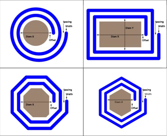
Note: Various coil shapes are available including Round, Rectangle, Octagon, and Hexagon.
Step 4: Specify the coil parameters.
Note: The following parameters are adjustable in the coil design:
- Width: Specifies the width of the trace used in the spiral inductor.
- Spacing: Specifies the spacing between traces in the spiral inductor.
- Diam X: Specifies the size of the spiral inductor in the X Direction.
- Diam Y: Specifies the size of the spiral in the Y Direction. This option is only available for rectangular shape.
- Turns: Specifies the number of turns in the spiral inductor.
- Rotation: Specifies the angle of rotation for the spiral inductor.
- Scale: The entire structure can be scaled by entering a value in the Scale field. This multiplies width, spacing, X diameter, and Y diameter in one step.
- Clockwise: Enabling Clockwise will mirror the structure along the Y-axis.
Once a parameter is changed, the coil will be recalculated and displayed within the form.
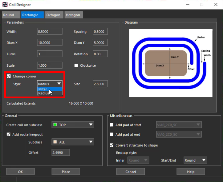
Step 5: Enable the Change corner option.
Note: This option is only available for the rectangular spiral pattern.
Step 6: From the Style drop-down menu, select Miter.
Note: This will add a miter to each corner of the rectangle. Selecting Round will round the corners of the rectangular spiral.
Step 7: In the Size field, enter a miter size of 2.5.
Note: If round was selected as the corner style, define a radius size.
Step 8: In the General section, specify the layer on which the spiral inductor will be drawn. Select Top.
Step 9: Select Add Route Keepout.
Note: This will automatically create a route keepout on the specified subclass.
Step 10: Set the Subclass as ALL and the Offset as 2.499.
Step 11: In the Miscellaneous section, specify if a padstack should be added to the start or endpoint of the spiral inductor.
Step 12: Select Convert Structure to Shape and set the Endcap Style to Round.
Note: This converts the spiral into one single static shape. If this is not checked, the spiral pattern will be realized as a sequence of cline segments.
Placing Coils on the PCB
Step 13: Select Place.
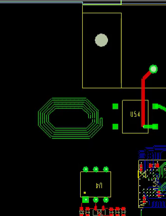
Step 14: Click to place the coil in the PCB canvas.
Step 15: Select OK to close the Coil Designer window.
Wrap up & Next Steps
Streamline the design and implementation of spiral inductors in RF and power applications with the easy-to-use, integrated Coil Designer in Allegro Productivity Toolbox. Learn more about the time-saving features of Productivity Toolbox with our free webinar.

