Sometimes the PCB Designer won’t have access to the source schematic files, making it more difficult to layout the PCB based on schematic connectivity. Reviewing a PDF of the schematic to determine the supporting circuitry and ideal PCB placement and manually locating the component in the PCB layout can be time-consuming. Quickly group components using a PDF of the schematic to optimize the PCB layout with the PCB Clustering App in OrCAD PCB Designer.
This how-to will provide step-by-step instructions on how to use the PCB Clustering App in OrCAD PCB Designer to efficiently group components using a PDF of the schematic.
To follow along with this tutorial, use the provided design above the table of contents.
How-To Video
Configuring PCB Clustering
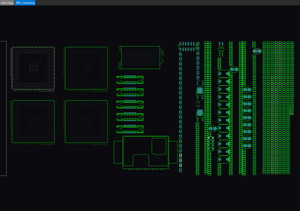
Step 1: Open the provided design, pdf_ clustering.brd, in OrCAD PCB Designer.
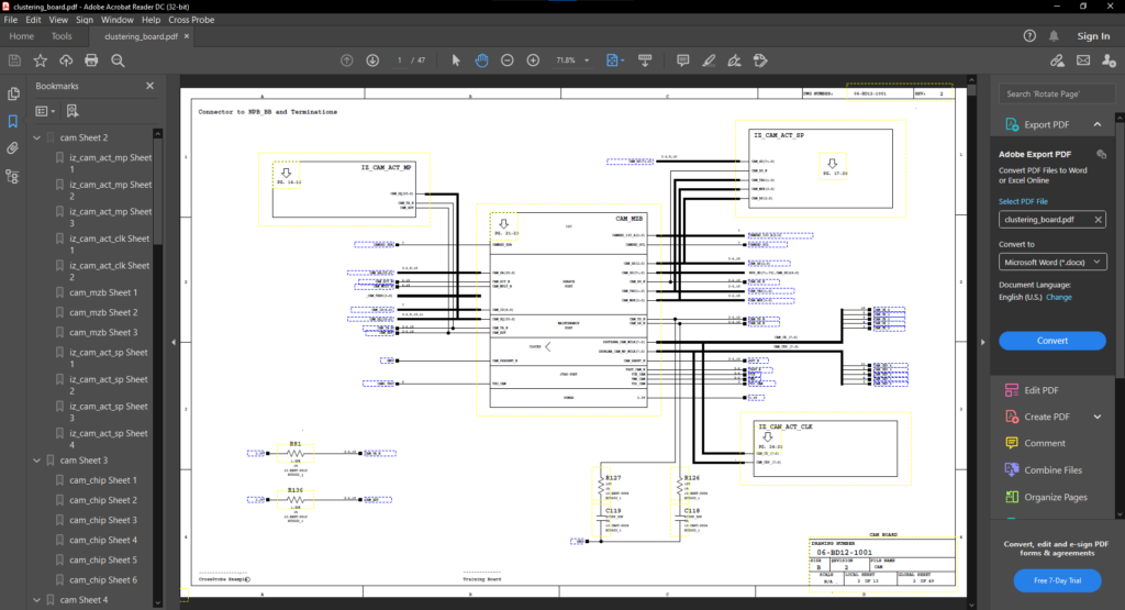
Step 2: Open the provided PDF, clustering_board.pdf in Adobe Acrobat Reader DC.
Note: The cross-probe functionality is only available in Adobe Acrobat Reader DC. If Adobe Acrobat DC opens by default, right-click on the PDF and select Open With > Adobe Acrobat Reader DC.
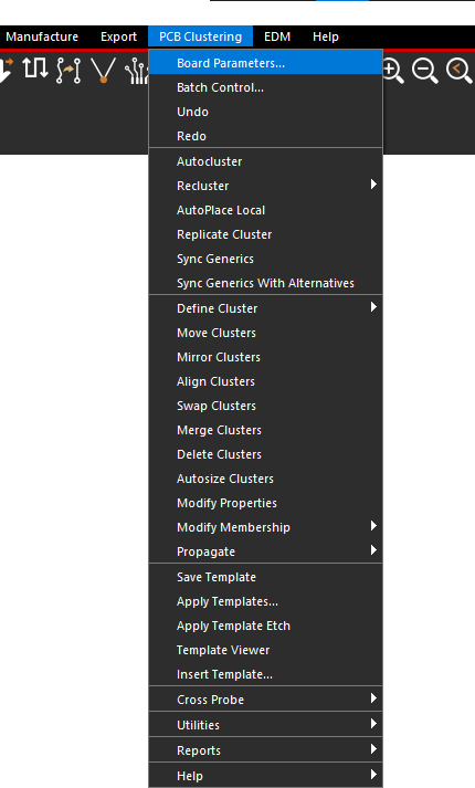
Step 3: In OrCAD PCB Designer, select PCB Clustering > Board Parameters from the menu.
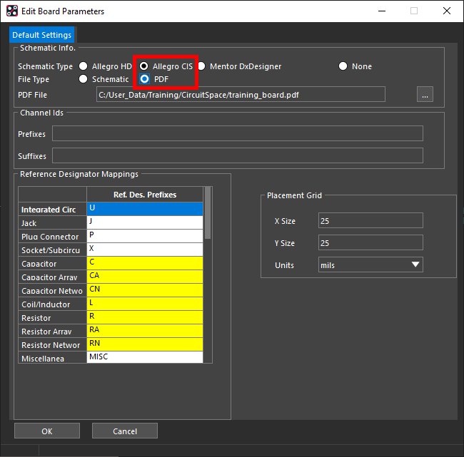
Step 4: The Edit Board Parameters window opens. Select Allegro CIS as the Schematic Type and PDF as the File Type.
Step 5: Select the ellipsis for PDF file to associate the PDF file.
Step 6: Browse to the location of the clustering_board.pdf. Select the file and click Open.
Step 7: Click OK to save the board parameters and close the window.
Activating Cross-Probe Functionality
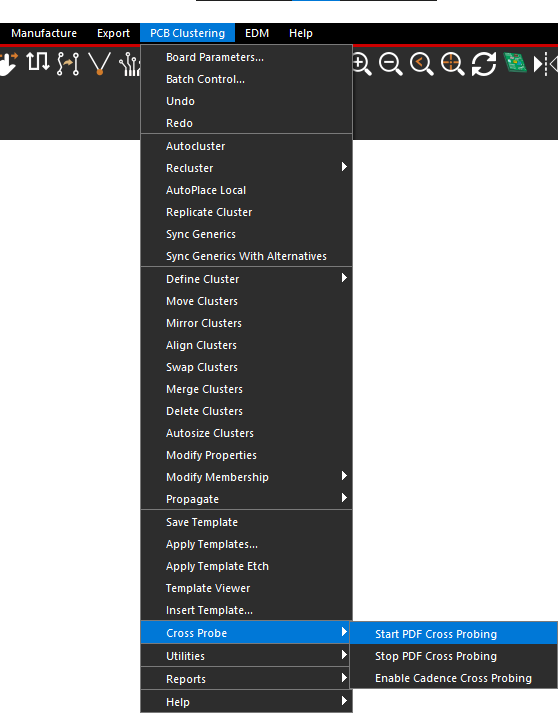
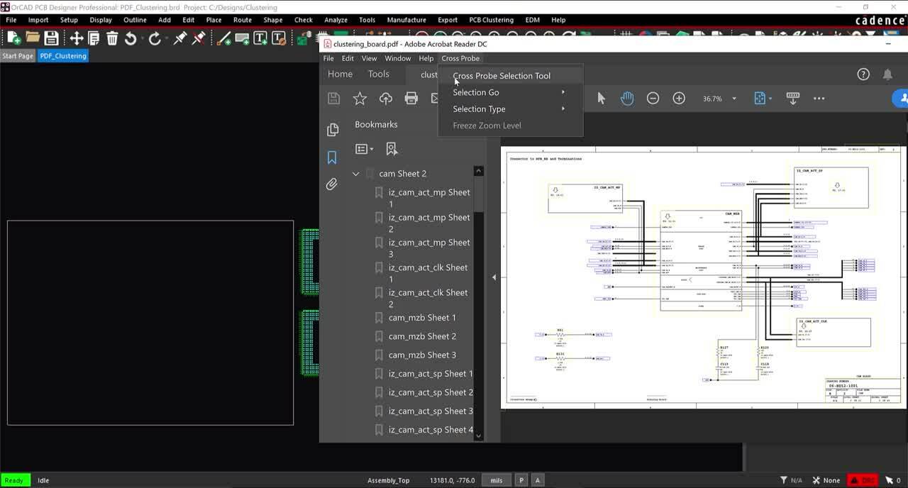
Step 8: Select PCB Clustering > Cross Probe > Start PDF Cross-Probing from the menu.
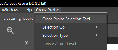
Step 9: In Adobe Acrobat Reader DC, select Cross Probe > Cross Probe Selection Tool.
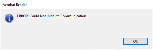
Note: If you receive an error message that communication could not initialize, select Edit > Preferences in Adobe Acrobat Reader DC. Under Categories, select Security (Enhanced). Uncheck Enable Protected Mode at Startup and click OK. Close Adobe Acrobat Reader DC and reopen the PDF.
PDF Component Selection
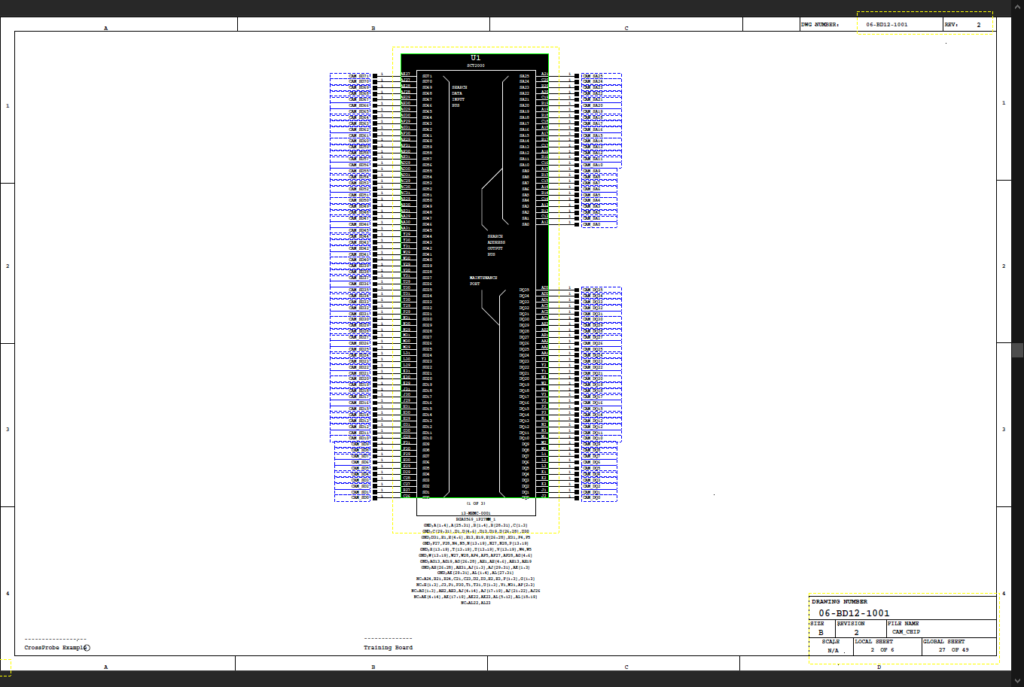
Step 10: Navigate to Cam Sheet 3 and select cam_chip Sheet 2. Click to select U1.
Step 11: Select page cam_chip Sheet 3. Hold down the CTRL key and click to select RA21.
Step 12: Select page cam_chip Sheet 4. Hold down the CTRL key and drag to select RA24 and RA22. Hold down the CTRL key and drag to select C699, C695, and R156.
Step 13: Select page cam_chip Sheet 5. Hold down the CTRL key and drag to select all the capacitors.
Step 14: Select page cam_chip Sheet 6. Hold down the CTRL key and drag to select all the capacitors.
Note: With selection in the PDF, the component is selected and zoomed into in the PCB canvas.
Automatic Component Grouping
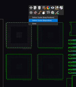
Step 15: When all the components have been selected in the PDF, return to OrCAD PCB Designer. Right-click in the PCB canvas and select Define Cluster (Reposition).
Note: Select Keep Position if the layout and/or routing is already completed. This process can be utilized when creating templates to reuse IP as templates can replicate placement, routing, and shapes.
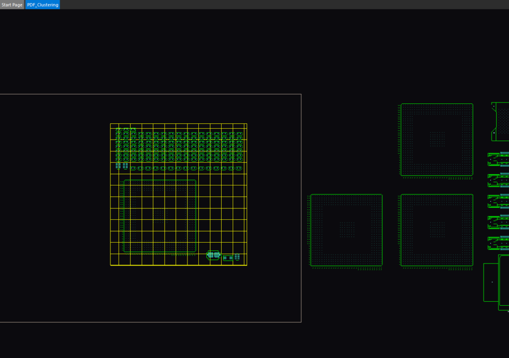
Step 16: Click to place the cluster on the PCB canvas.
Wrap Up & Next Steps
Efficiently layout the PCB design by quickly clustering components using a PDF of the schematic with the PCB Clustering App. This app and others are part of the EMA Toolkit, one of the benefits of EMA Support +. The EMA Support + program is available to all EMA customers on active support and includes additional benefits and tools to expedite the PCB design process, such as time saving apps, additional training, and more. See what’s included with EMA Support + and learn how to get access to these exclusive benefits.

