In today’s high-speed designs, the importance of component placement can’t be overstated. The location of a decoupling capacitor, passive component on a differential pair, and even the length of a trace can make the difference between a functional and non-functional design. Poor component placement can complicate the PCB layout, requiring additional routing, vias, and space that may not be available. Streamline the PCB layout process and automatically place components based on schematic connectivity with the PCB Clustering App.
This how-to will provide step-by-step instructions on how to use the PCB Clustering App in OrCAD PCB Designer to automatically cluster and place components based on the schematic.
To follow along with this tutorial, download and extract the provided design above the table of contents.
How-To Video
Configuring PCB Clustering
Step 1: Open the provided design in OrCAD PCB Designer.
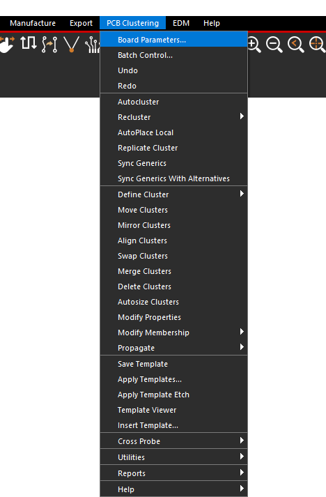
Step 2: Select PCB Clustering > Board Parameters from the menu.
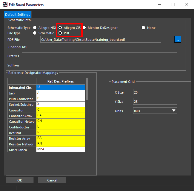
Step 3: Select Allegro CIS as the Schematic Type.
Step 4: Select PDF as the File Type.
Step 5: Select the ellipsis to change the PDF File.
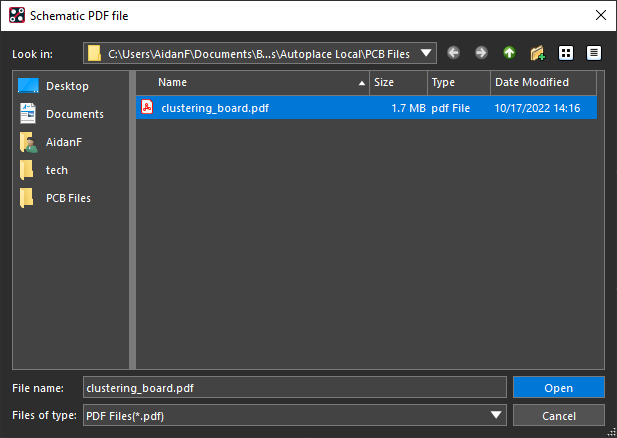
Step 6: Browse to the location of the clustering_board.pdf file. Select the file and click Open.
Step 7: Click OK to save the settings and close the window.
Automatically Cluster Components
Step 8: Select PCB Clustering > Autocluster from the menu.
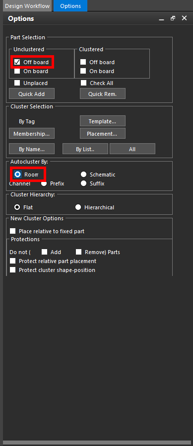
Step 9: Under Part Selection, select Unclustered > Off Board.
Step 10: Under Autocluster By, select Room.
Note: This design has room properties already configured. In future designs this can be achieved by defining the Room property for each component in OrCAD Capture.
Step 11: Right-click anywhere in the PCB canvas and select Done.
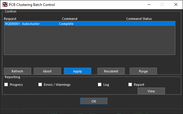
Step 12: The PCB Clustering Batch Control window opens. Select Apply and OK.
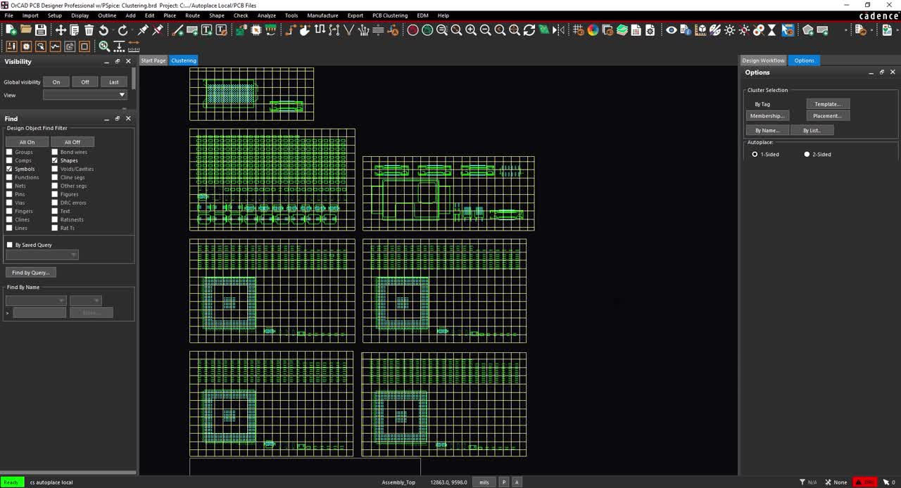
Automatically Place Components
Step 13: Select PCB Clustering > Autoplace Local from the menu.
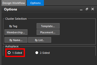
Step 14: Under Autoplace, select 1-sided.
Note: To place components on both the top and bottom sides of the PCB, select 2-sided.
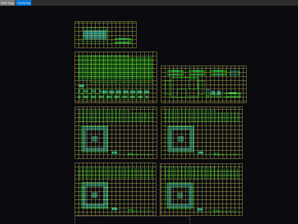
Step 15: Click to select each cluster. Right-click in the PCB canvas and select Done.
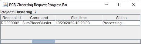
Note: The PCB Clustering Request Progress Bar may appear while the PCB Clustering App is determining the best component placement for the selected clusters.
Applying Component Placement
Step 16: The PCB Clustering Batch Control window will open, with an Autoplace Local control highlighted. Select Apply and OK.
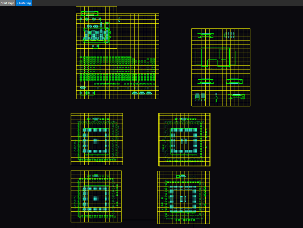
Step 17: View the results. The components have been automatically placed based on schematic connectivity.
Wrap Up & Next Steps
Quickly place components by connectivity with automatic placement based on schematic connections using the PCB Clustering App. This app and others are part of the EMA Toolkit, one of the benefits of EMA Support +. The EMA Support + program is available to all EMA customers on active support and includes additional benefits and tools to expedite the PCB design process, such as time saving apps, additional training, and more. See what’s included with EMA Support + and learn how to get access to these exclusive benefits.

