Today’s fast-paced market creates timelines for PCB design which are difficult to achieve. Reusing known-good and verified sections of circuitry can streamline the design process. With the PCB Clustering App in OrCAD PCB Designer, easily replicate component placement, routing, and shapes with templates to quickly layout similar circuitry and accelerate the PCB design process.
This how-to will provide step-by-step instructions on how to use the PCB Clustering App in OrCAD PCB Designer to replicate component placement with templates.
To follow along with this tutorial, use the provided design above the table of contents.
How-To Video
Creating a Template
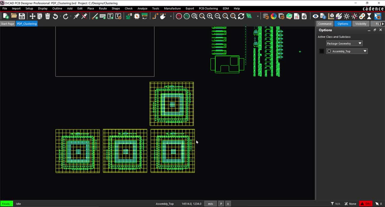
Step 1: Open the provided design, clustering_template.brd, in OrCAD PCB Designer.
Step 2: Select PCB Clustering > Save Template from the menu.
Step 3: Select the groups clustered components. Right-click in the PCB canvas and select Done.
Step 4: Browse to the location to save the template or use the default location.
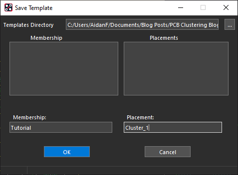
Step 5: Enter Tutorial for the Membership and Cluster_1 for the Placement. Click OK.
Applying a Template
Step 6: Select PCB Clustering > Apply Templates from the menu.
Note: If the template was saved in a different location other than the default, browse to the same location to apply the template.
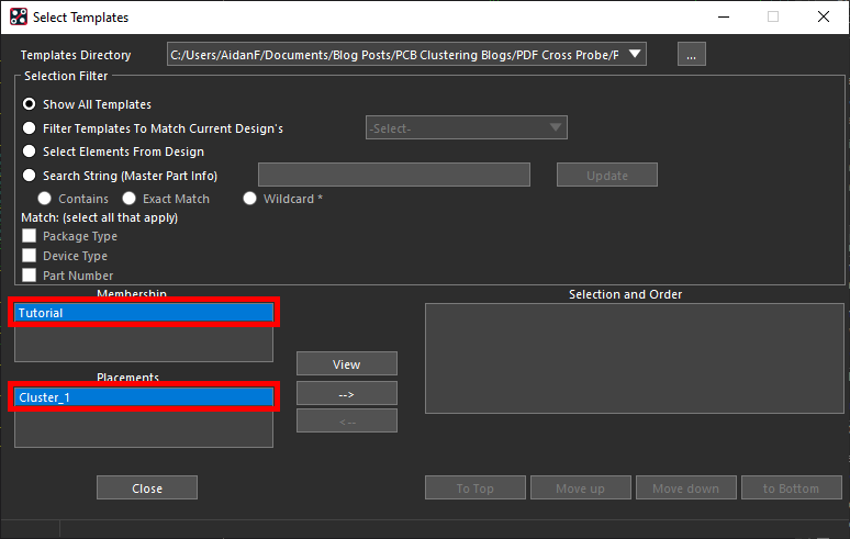
Step 7: Under Membership, select Tutorial.
Step 8: Under Placement, select Cluster_1.
Step 9: Click the arrow (–>) to select the template.
Step 10: Select View to preview the template. Close the preview.
Step 11: In the Select Templates window, select Close.
Replicate Component Placement
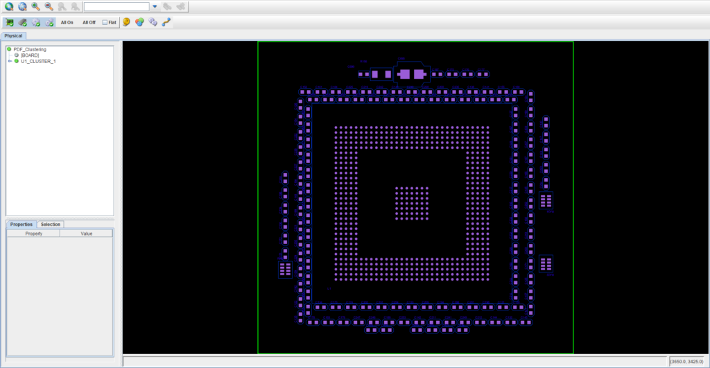
Step 12: Right-click on the PCB canvas and select Done.
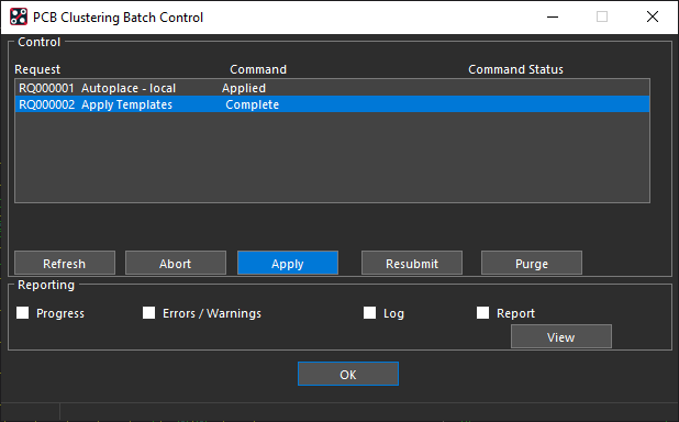
Step 13: The PCB Clustering Batch Control window opens. Select Apply and OK to apply the changes.
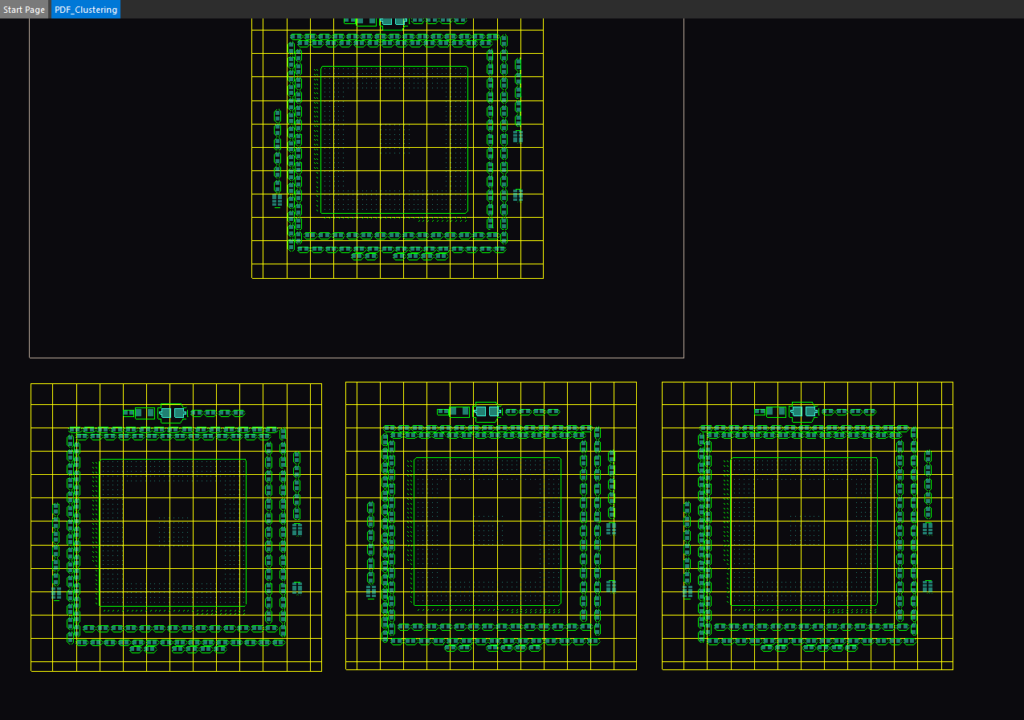
Step 14: View the clusters. The PCB Clustering App has analyzed the components in the design and automatically applied the template.
Wrap Up & Next Steps
Quickly replicate component placement for similar circuitry and accelerate the PCB layout with templates in the PCB Clustering App. This app and others are part of the EMA Toolkit, one of the benefits of EMA Support +. The EMA Support + program is available to all EMA customers on active support and includes additional benefits and tools to expedite the PCB design process, such as time saving apps, additional training, and more. See what’s included with EMA Support + and learn how to get access to these exclusive benefits.

