
Activating the Constraints Panel in OrCAD X Presto
Step 1: Open the provided design in OrCAD X Presto Professional.
Step 2: If the Constraints panel is not visible, select View > Panels > Constraints from the menu. This panel provides an easy-to-use interface containing visual graphics to aid in the definition and assignment of rules directly in the PCB canvas.
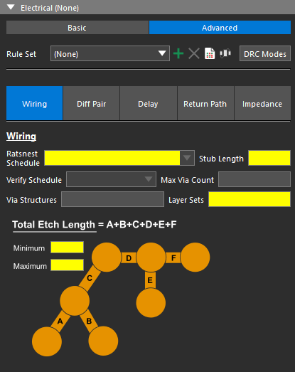
Step 3: Basic constraints are visible for Electrical, Physical, Spacing, and Same Net Spacing. Select Advanced under Electrical to define advanced electrical rules including:
- Wiring
- Differential Pair
- Propagation Delay
- Return Path
- Impedance
Step 4: Select Impedance to define an impedance rule set.
Creating an Electrical CSet
Step 5: Select the plus sign for Create Electrical CSet to create a new constraint set.
Step 6: The Create Electrical CSet window opens. Enter BNC for the name.
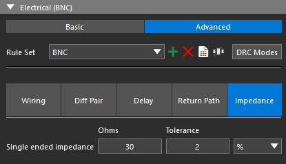
Step 7: Click OK. The constraint set is automatically selected from the Rule Set dropdown.
Step 8: For Single-ended Impedance, enter 30 for the target impedance and 2% for the tolerance.
Assigning an Electrical CSet
Step 9: The constraint set must be assigned to the appropriate nets before they can be checked. In the Selection Filter subpanel, deselect All Objects and select Nets to allow the selection of nets.
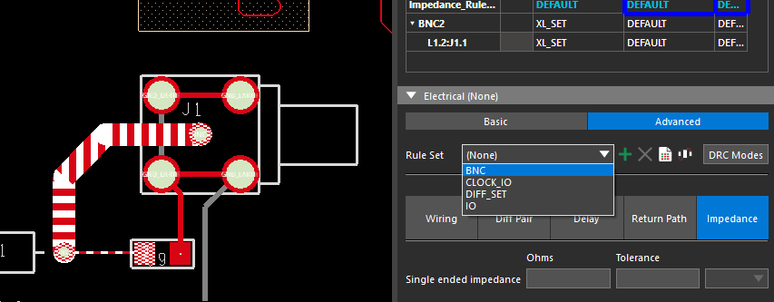
Step 10: Select a pin or trace on the BNC2 net in the PCB canvas. In the Constraints panel, select BNC from the Rule Set dropdown to assign the constraint set.
Step 11: Constraints can also be defined and assigned in the Constraint Manager. Select the constraint manager icon in the constraints panel or Electrical Analysis > Constraint Manager from the menu to activate the Constraint Manager.
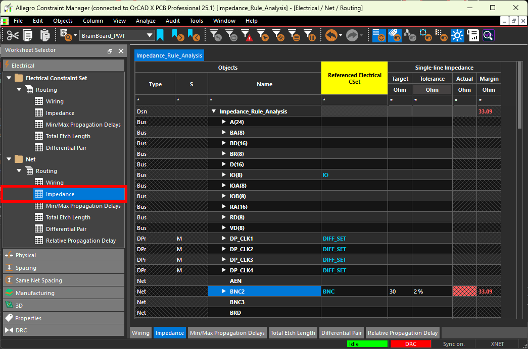
Step 12: The Constraint Manager window opens, showing a directory of constraint domains and worksheets. Constraints and constraint sets can be created, defined and assigned in the constraint manager. To assign the previously created CSet, select the Electrical domain and the Net > Routing > Impedance worksheet.
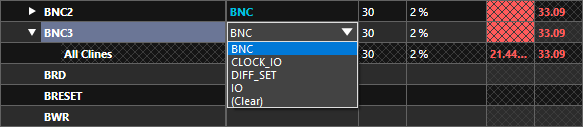
Step 13: Select the cell under Referenced Electrical CSet for net BNC3 and select constraint set BNC from the resulting dropdown. The defined impedance constraints are assigned to nets BC2 and BC3 and analysis is automatically activated.
Verify Design Rule Check Activation
Step 14: Select Analyze > Analysis Mode from the Constraint Manager menu.
Step 15: The Analysis Modes window opens. Here you can enable all design rule checks available in OrCAD X. Select Electrical from the list on the left.
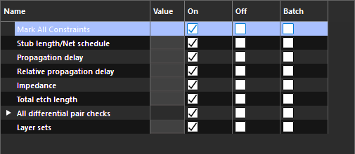
Step 16: Ensure On is selected for Mark All Constraints to enable all electrical rule checks.
Step 17: Click OK to save the settings and close the window.
Step 18: View the measured impedance for both BNC connectors in the Constraint Manager. The impedance values are listed in red, indicating that they are out of range and failing.
Correcting Impedance Constraint Violations
Step 19: Minimize the Constraint Manager.
Step 20: Select Properties to open the Properties panel. The DRC pie chart shows there are 10 impedance rules in violation in the PCB. Select the DRC pie chart to open a list of design rule violations in the Search panel.
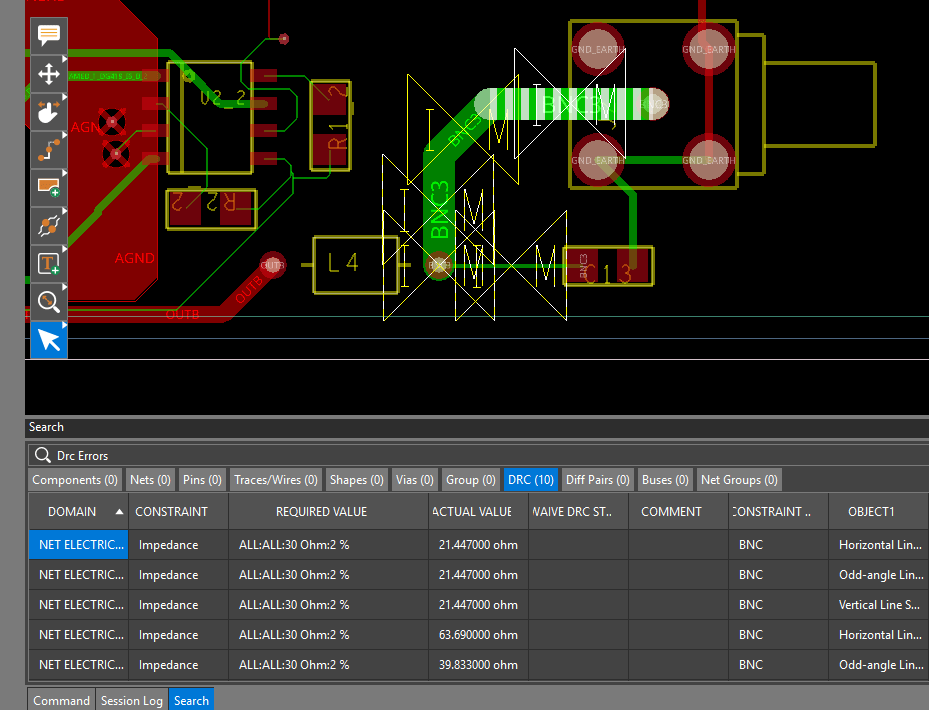
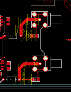
Step 21: Double-click a violation to be brought to its location in the canvas. The trace widths can be changed to adjust the impedance.
Step 22: Enable Traces in the Selection Filter subpanel to allow the selection of traces. Deselect Nets.
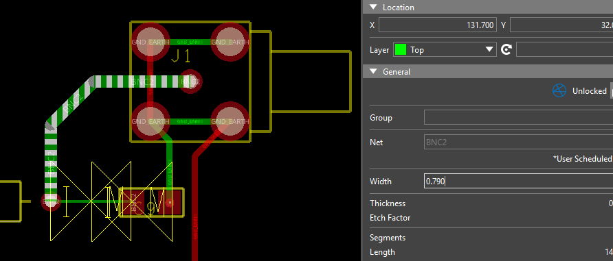
Step 23: Select one of the affected traces. In the Properties panel, set the trace width to 0.790, which was calculated as the appropriate line width to meet impedance requirements.
Step 24: Repeat this process for all affected traces with impedance DRC markers.
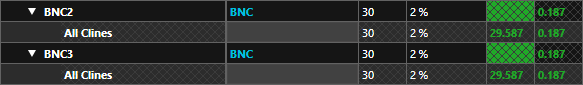
Step 25: Reopen the Constraint Manager. The impedance values are now listed in green, indicating that the trace impedances are now within spec.
Activating the Constraints Panel in OrCAD X PCB Editor
Step 1: Open the provided design in OrCAD X PCB Designer Professional.
Step 2: If the Constraints panel is not visible, select Display > Windows > Constraints from the menu.
Step 3: The Constraints panel opens on the right side of the PCB canvas. Select Advanced under Electrical to define advanced electrical rules including:
- Wiring
- Differential Pair
- Propagation Delay
- Return Path
- Impedance
Step 4: Select Impedance to define an impedance rule set.
Creating an Electrical CSet
Step 5: Select the plus sign for Create Electrical CSet to create a new constraint set.
Step 6: The Create Electrical CSet window opens. Enter BNC for the name.
Step 7: Click OK. The constraint set is automatically selected from the Rule Set dropdown.
Step 8: For Single-ended Impedance, enter 30 for the target impedance and 2% for the tolerance.
Assigning an Electrical CSet
Step 9: The constraint set must be assigned to the appropriate nets before they can be checked. In the Find panel, select All Off and check Nets to allow the selection of nets.
Step 10: Select a pin or trace on the BNC2 net in the PCB canvas. In the Constraints panel, select BNC from the Rule Set dropdown to assign the constraint set.
Step 11: Constraints can also be defined and assigned in the Constraint Manager. Select the Constraint Manager icon in the Constraints panel or Setup > Constraints from the menu to activate the Constraint Manager.

Step 12: The Constraint Manager window opens, showing a directory of constraint domains and worksheets. Constraints and constraint sets can be created, defined and assigned in the constraint manager. To assign the previously created CSet, select the Electrical domain and the Net > Routing > Impedance worksheet to assign the constraint set.
Step 13: Select the cell under Referenced Electrical CSet for net BNC3 and select constraint set BNC from the resulting dropdown. The defined impedance constraints are assigned to nets BC2 and BC3 and analysis is automatically activated.
Verify Design Rule Check Activation
Step 14: Select Analyze > Analysis Mode from the Constraint Manager menu.
Step 15: The Analysis Modes window opens. Here you can enable all design rule checks available in OrCAD X PCB Designer. Select Electrical from the list on the left.

Step 16: Ensure On is selected for Mark All Constraints to enable all electrical rule checks.
Step 17: Click OK to save the settings and close the window.
Step 18: View the measured impedance for both BNC connectors in the Constraint Manager. The impedance values are listed in red, indicating that they are out of range and failing.
Correcting Impedance Constraint Violations
Step 19: Minimize the Constraint Manager.
Step 20: Scroll up to zoom into the BNC connectors at the bottom of the board. The trace widths can be changed to adjust the impedance.
Step 21: Select Edit > Change Objects from the menu.
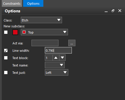
Step 22: In the Options panel, check the option for Line Width and enter 0.790 into the Line Width field. This was calculated as the appropriate line width to meet impedance requirements.
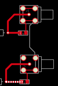
Step 23: Click the traces on the BNC nets to change the widths. The DRC markers are automatically removed. When finished, right-click and select Done.
Step 24: Reopen the Constraint Manager. The impedance values are now listed in green, indicating that the trace impedances are now within spec.

