
Activating the Constraints Panel
Step 1: Open the provided design in OrCAD X Presto. OrCAD X includes a constraints panel, allowing designers to define and assign constraint sets directly on the PCB canvas.
Step 2: Select View > Panels > Constraints to open the Constraints panel if it is not already open.
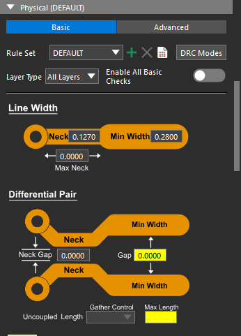
Step 3: The Constraints panel opens on the right side of the canvas with the Options panel. Scroll to Physical to define physical constraint sets.
Defining Physical Rules in OrCAD X Presto
Step 4: Select the plus sign for Create Physical CSet to create a new constraint set.
Step 5: The Create Physical CSet window opens. Enter POWER_GND for the name.
Step 6: Click OK. The constraint set is automatically selected in the Rule Set dropdown.
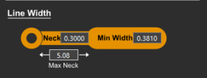
Step 7: Scroll to the physical constraint set graphic. Enter 0.381 for the Minimum Line Width, 0.3 for the Minimum Neck Width, and 5.08 for the Maximum Neck Length.
Step 8: Scroll to the Via List table to define acceptable vias. From this table, you can select the via padstacks allowed on nets assigned the constraint set.
Step 9: Select the Edit Via List Dialog button on the right side of the panel. The Edit Via List window opens.
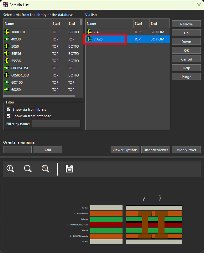
Step 10: In the via selection table, scroll down and double-click VIA26 to add the via to the list. Click OK.
Step 11: View the Via List table. Vias VIA and VIA26 are now listed, indicating they can both be used in the design.
Assigning Physical Rules to Nets in OrCAD X Presto
Step 12: In the Selection Filter subpanel, disable All Objects and enable Nets to allow the selection of nets.
Step 13: Select a pin or trace on the 3.3V net in the PCB canvas. These nets are highlighted in purple for easy identification.

Step 14: In the Constraints panel, select POWER_GND from the Rule Set dropdown to assign the constraint set. Click anywhere in the canvas to deselect the net.
Step 15: Constraints can also be defined and assigned in the Constraint Manager. Select Electrical Analysis > Constraint Manager from the menu to activate the Constraint Manager.
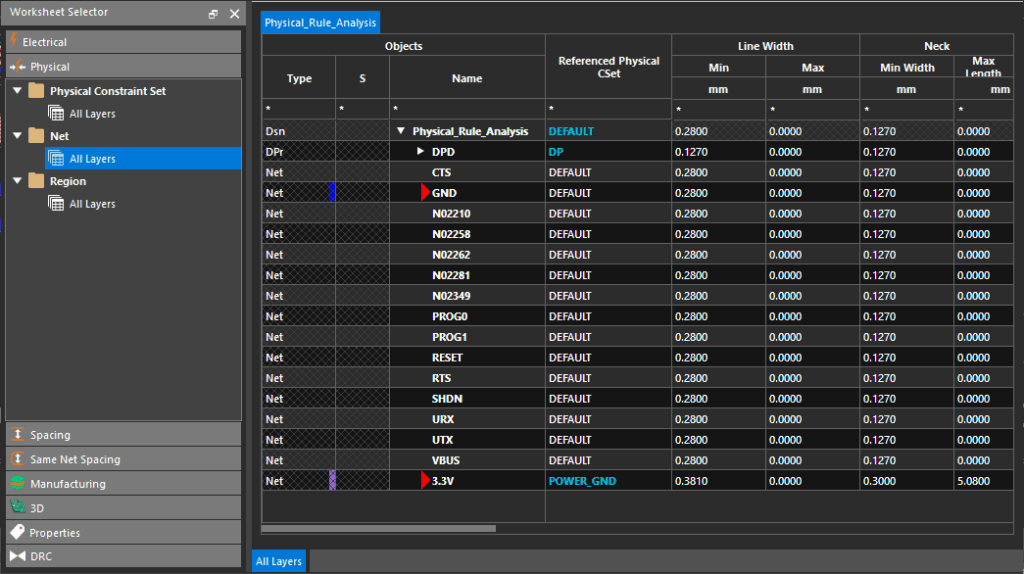
Step 16: The Constraint Manager window opens, showing a directory of constraint domains and worksheets. Select Physical > Net > All Layers. Rules can be assigned to individual nets here, but to save time groups of rules can be created and assigned to nets with constraint sets.
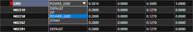
Step 17: Select the cell under Referenced Physical CSet for the GND net and choose POWER_GND from the resulting dropdown. The constraints defined in the Constraints panel are listed.
Step 18: Close the Constraint Manager.
Verifying Adherence to Physical Rules in OrCAD X Presto
Step 19: The DRC cache must be updated to report any physical constraint violations. Select Properties on the right side of the window to open the Properties panel if it is not already open.
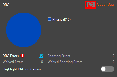
Step 20: Select Refresh in the DRC section of the Status subpanel in the Properties panel to update the DRC pie chart.
Step 21: Click the pie chart to open a list of DRC violations in the Search panel.
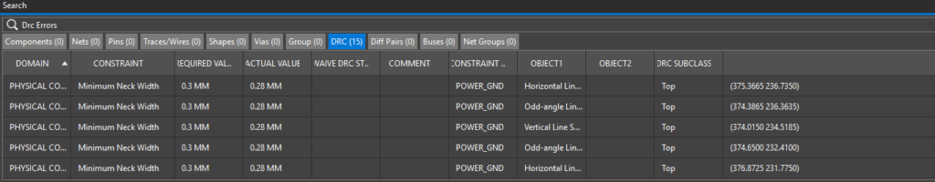
Step 22: View the list in the Search panel. The errors indicate that the power/ground traces throughout the board are thinner than the assigned constraints require.
Step 23: Double-click a violation to be brought to its location on the board.
Correcting Physical Constraint Violations
Step 24: In the Selection Filter subpanel of the Properties panel, select All Objects twice to turn all objects off and select Traces to enable the selection of traces.
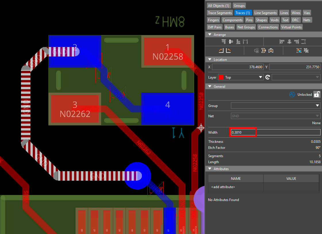
Step 25: Select an affected trace. In the Properties panel, set the width to 0.381. The error marker is removed.
Step 26: Repeat step 25 for all marked traces in the design. When finished, click a blank area of the canvas to view the general Properties panel.
Step 27: View the DRC section of the Status subpanel. All physical DRC violations have been cleared.
Activating the Constraints Panel
Step 1: Open the provided design in OrCAD X PCB Designer. OrCAD X includes a constraint panel, allowing designers to define and assign constraint sets directly on the PCB canvas.
Step 2: Select Display > Windows > Constraints to open the Constraints panel.
Step 3: The Constraints panel opens on the right side of the canvas with the Options panel. Scroll to Physical to define physical constraint sets.
Defining Physical Rules in OrCAD X PCB Designer
Step 4: Select the plus sign for Create Physical CSet to create a new constraint set.
Step 5: The Create Physical CSet window opens. Enter POWER_GND for the name.
Step 6: Click OK. The constraint set is automatically selected in the Rule Set dropdown.
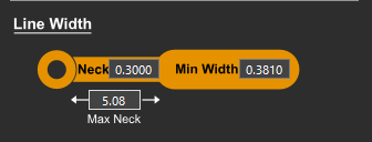
Step 7: Scroll to the physical constraint set graphic. Enter 0.381 for the Minimum Line Width, 0.3 for the Minimum Neck Width, and 5.08 for the Maximum Neck Length.
Step 8: Scroll to the Via List table to define acceptable vias. From this table, you can select the via padstacks allowed on nets assigned the constraint set.
Step 9: Select the Edit Via List Dialog button on the right side of the panel. The Edit Via List window opens.
Step 10: In the via selection table, scroll down and double-click VIA26 to add the via to the list. Click OK.
Step 11: View the Via List table. Vias VIA and VIA26 are now listed, indicating they can both be used in the design.
Assigning Physical Rules to Nets in OrCAD X PCB Designer
Step 12: In the Find panel, select All Off and check Nets to allow the selection of nets.
Step 13: Select a pin or trace on the 3.3V net in the PCB canvas. These nets are highlighted in purple for easy identification.
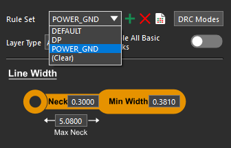
Step 14: In the Constraints panel, select POWER_GND from the Rule Set dropdown to assign the constraint set.
Step 15: Constraints can also be defined and assigned in the Constraint Manager. Select Setup > Constraints from the menu to activate the Constraint Manager.
Step 16: The Constraint Manager window opens, showing a directory of constraint domains and worksheets. Select Physical > Net > All Layers. Rules can be assigned to individual nets here, but to save time groups of rules can be created and assigned to nets with constraint sets.
Step 17: Select the cell under Referenced Physical CSet for the GND net and choose POWER_GND from the resulting dropdown. The constraints defined in the Constraints panel are listed.
Step 18: Close the Constraint Manager.
Verifying Adherence to Physical Rules in OrCAD X PCB Designer
Step 19: The DRC cache must be updated to report any physical constraint violations. Select Check > Design Status from the menu.
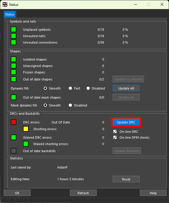
Step 20: The Status window opens. The DRC Errors marker is red, indicating that the cache is out of date. Select Update DRC.
Step 21: The DRC Errors marker is now yellow, indicating that the cache is up to date and there are errors present. Click the marker to open a DRC report.
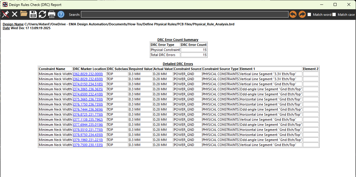
Step 22: View the DRC report. The listed errors indicate that the power/ground traces throughout the board are thinner than the assigned constraints require.
Step 23: Click a link under DRC Marker Location to be brought to the location of the associated error. Close the DRC report.
Step 24: Click OK to close the Status window.
Correcting Physical Constraint Violations
Step 25: To correct these violations, the power and ground traces must be widened. Select Edit > Change Objects from the menu.
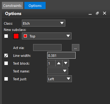
Step 26: Select the Options tab. In the Options panel, check the option for Line Width and enter 0.381.
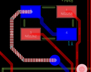
Step 27: Click each of the thin traces on the PCB canvas to thicken them and remove the DRC markers. When finished, right-click and select Done.
Step 28: To confirm the fixes, select Check > Design Status from the menu.
Step 29: View the Status window. Select Update DRC if required. The DRC Errors marker is now green, indicating no violations. All violations of the defined physical constraints have been corrected.

