
Check the Artwork Films
Step 1: Open a design in OrCAD X. For this how-to a reference design with artwork films fully defined is provided as an example. If there are no artwork films for the loaded board, they must be defined before a PDF can be generated. Get the step-by-step how-to here.
Step 2: In OrCAD X, PDF documentation is created as part of the manufacturing documentation. Select Manufacturing > Export to Manufacturing from the menu.
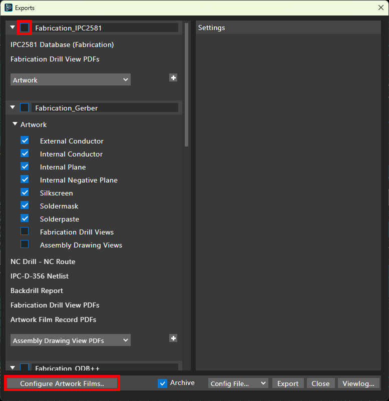
Step 3: The Exports window opens, showing the available forms to export. Uncheck the option for Fabrication_IPC2581.
Step 4: Artwork films should be checked and verified before a PDF is generated. Select Configure Artwork Films at the bottom of the window.
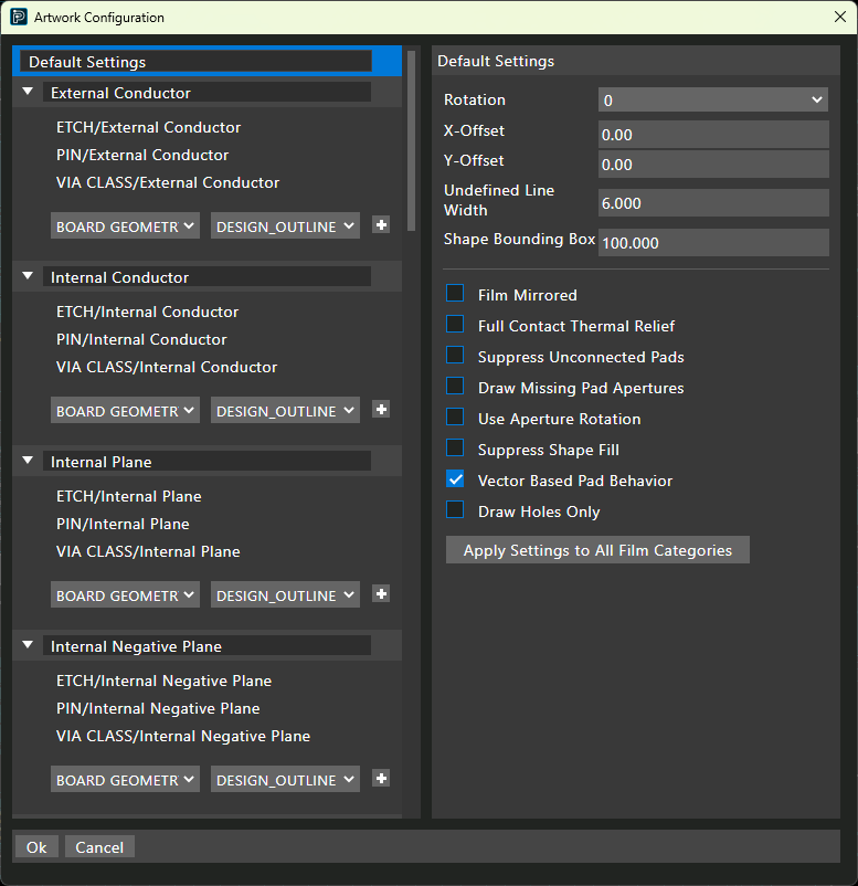
Step 5: Scroll through the list of artwork films in the design. All required films are present and will be printed to the PDF. Click OK to return to the Exports window.
Define the PDF Export
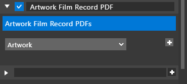
Step 6: To define the PDF export, scroll to the bottom of the window to the empty field. Enter Artwork Film Record PDF and click the plus sign to create the export category.
Step 7: Select Artwork Film Record PDFs from the dropdown. Click the plus sign to add the PDF to the category.
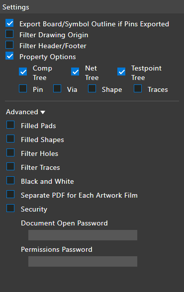
Step 8: Select the new entry. Configure the settings on the right side of the window as required.
Step 9: Uncheck the option for Archive to save the PDF directly in your working directory.
Step 10: Click Export. A prompt appears, saying that the current Gerber layer definitions will be replaced. Click OK to proceed.
Click Close to close the Exports window.
Viewing the PDF of your PCB
Step 11: Open File Explorer and browse to your working directory.
Step 12: The PDF if saved in a folder with the board name followed by “_Artwork_Film_Record_PDF.” Open the folder.
Step 13: Open the generated PDF file.
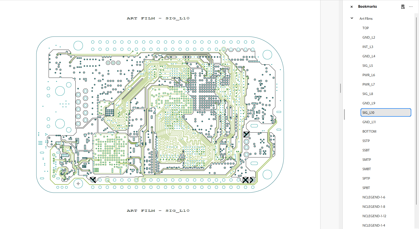
Step 14: Scroll through the PDF. Each artwork film is printed on its own page.
Step 15: Open the index in the PDF viewer to select the desired film to view. Select a film to view it.
Activate PDF Export
Step 1: Open a design in OrCAD X PCB Designer. For this how-to a reference design with artwork films fully defined is provided as an example.
Step 2: To activate PDF Export, select Export > PDF from the menu.
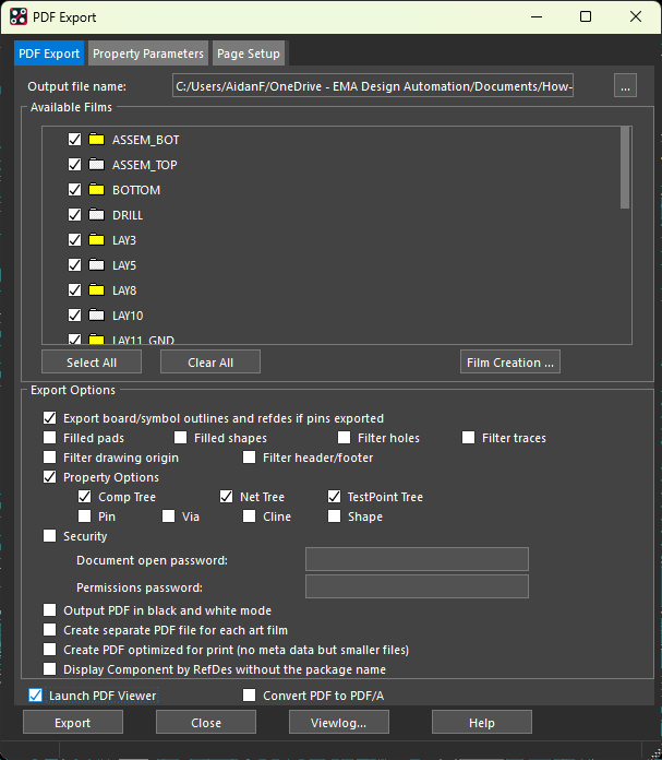
Step 3: The PDF Export window opens, showing the available PDF generation settings. Select the ellipsis for Output File Name.
Step 4: Browse to the working directory. Enter a name for the PDF and click Save.
Generate a PDF of your PCB
Step 5: None of the films are selected for export by default. Choose Select All under Available Films to select all available films.
Step 6: Check the options under Export Options as required for your PDF.
Step 7: To view the PDF when generation is finished, check Launch PDF Viewer.
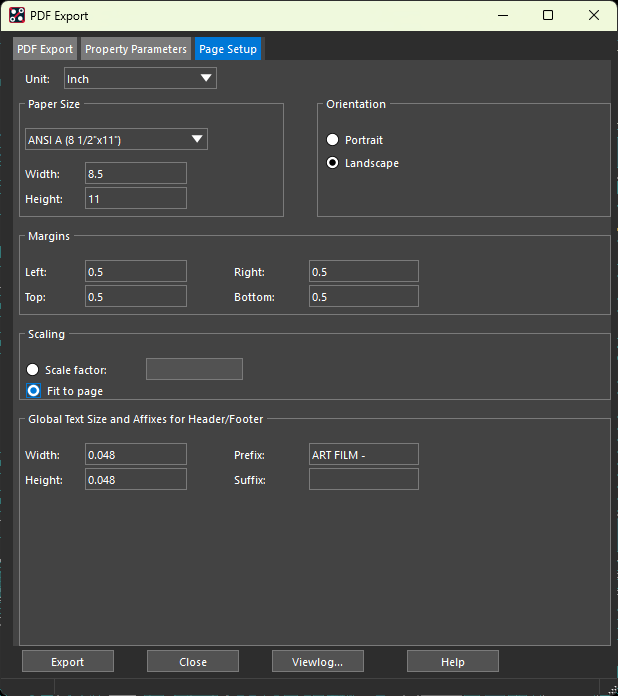
Step 8: Select the Page Setup tab to configure output page settings.
Step 9: To generate a standard US letter size PDF, select ANSI A (8½ × 11) from the Paper Size dropdown. For larger board sizes, select a larger size or enter custom dimensions.
Step 10: Since the example board is wider than it is tall, select Landscape for the Orientation.
Step 11: Select Fit to Page under Scaling to scale the board to fit the page size.
Step 12: Click Export. The PDF is generated and opens in your default PDF viewer when completed.
View the PDF of your PCB
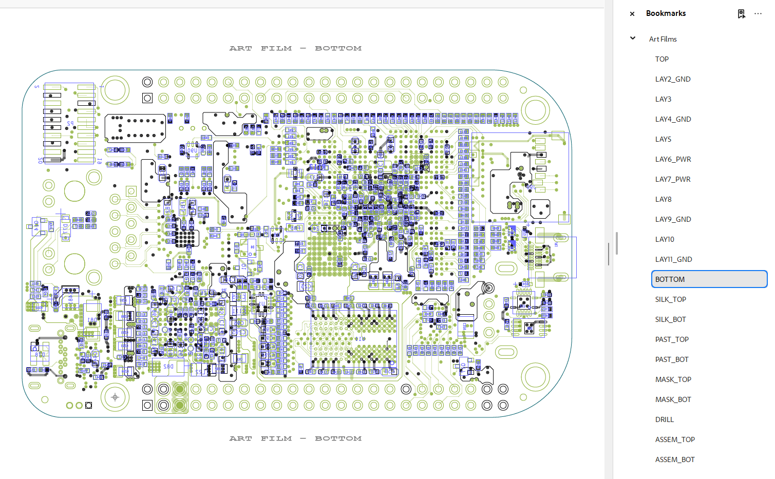
Step 13: Scroll through the PDF. Each artwork film is printed on its own page.
Step 14: Open the index in the PDF viewer to select the desired film to view. Select a film to view it.

