
Configuring Pad-Pad Constraints in OrCAD X
Step 1: Open the provided design in OrCAD X Presto Professional.
Step 2: OrCAD X includes a Constraints panel, allowing designers to define and assign constraint sets directly on the PCB canvas. Select View > Panels > Constraints to open the Constraints panel if it is not already open.
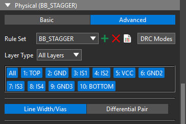
Step 3: The Constraints panel opens on the right side of the canvas. This provides an efficient method for defining and assigning electrical, physical, and spacing constraints with the aid of a visual graphic. Scroll down to Physical and select Advanced to define all physical constraints available in OrCAD X.
Defining Pad-Pad Rules in OrCAD X: Staggered Vias
Step 4: Select the plus sign for Create Physical CSet to create a new CSet.
Step 5: The Create Spacing CSet window opens. Enter BB_STAGGER for the name.
Step 6: Click OK. The constraint set is automatically selected in the Rule Set dropdown.
Step 7: The bottom of the Physical subpanel shows a list of vias that can be placed in the constraint set. Select Edit Via List Dialog to modify the list.
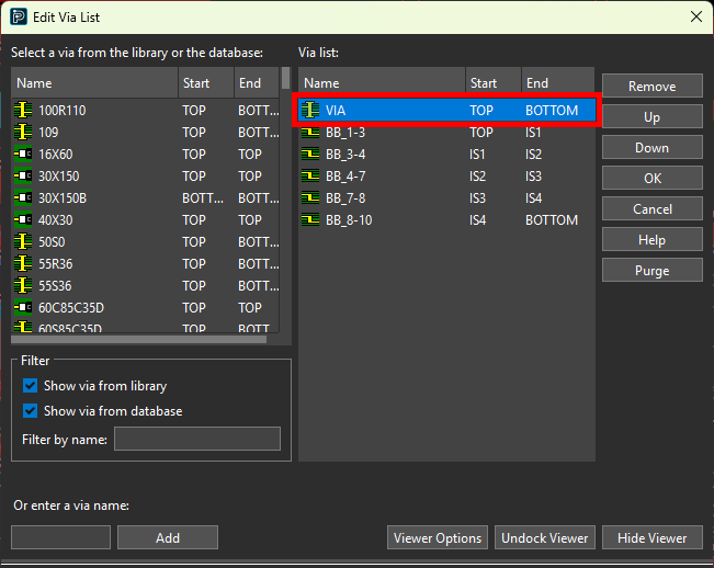
Step 8: By default, all blind and buried vias and the default via can be placed. To remove the default via, double-click it in the Via List.
Step 9: Click OK to save the settings and close the window. The default through-hole via is no longer listed in the Via List.
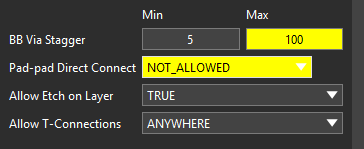
Step 10: Set the BB Via Stagger minimum to 5 and maximum to 100.
Defining Pad-Pad Rules in OrCAD X: Stacked Vias
Step 12: To create a rule set for stacked vias, select Create Physical CSet near the top of the subpanel again.
Step 13: Name the set BB_STACK and click OK.
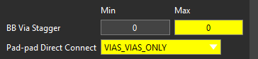
Step 14: Set the minimum and maximum BB Via Stagger to 0.
Step 15: Select VIAS_VIAS_ONLY from the Pad-Pad Direct Connect dropdown. This will allow pad-to-pad connections only between vias.
Assigning Pad-Pad Rules to Nets in OrCAD X
Step 16: Constraint sets can be assigned to groups of nets in the Constraint Manager. Select Electrical Analysis > Constraint Manager from the menu to activate the Constraint Manager.
Step 17: The Constraint Manager window opens, showing a directory of constraint domains and worksheets. Select the Physical domain and the Net > All Layers worksheet.
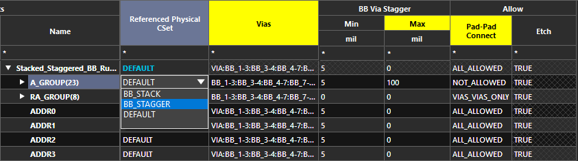
Step 18: Select the cell under Referenced Physical CSet for net group A_GROUP. Select BB_STAGGER from the dropdown. The stagger constraint set is assigned to all nets in the group.
Step 19: Select the cell under Referenced Physical CSet for net group RA_GROUP and assign the BB_STACK constraint set to the group.
Activating Design Rule Checks
Design rule checks must be activated for pad-pad connections before any violations are reported.
Step 20: Select Analyze > Analysis Mode from the Constraint Manager menu.
Step 21: The Analysis Modes window opens. Here you can enable all design rule checks available in OrCAD X. Select Physical from the list on the left.
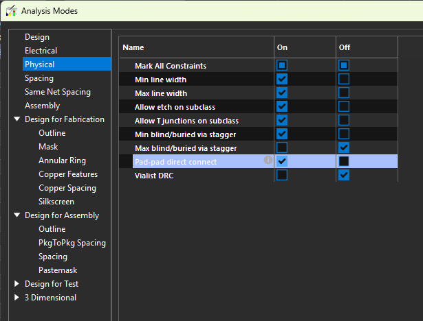
Step 22: Select On for Pad-Pad Direct Connect to enable rule checks for pad-pad connections.
Step 23: Click OK to save the settings and close the window.
Step 24: Close the Constraint Manager.
Verifying Adherence to Pad-Pad Rules in OrCAD X
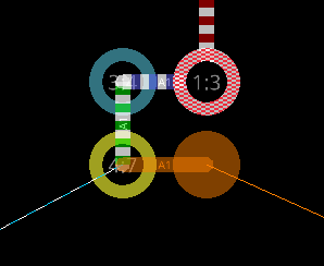
Step 25: Zoom into the unrouted pins of nets A1 and RA0 on U10, indicated by ratsnest lines.
Step 26: Select the Add Connect mode from the toolbar.
Step 27: Select net A1 to start routing. Select Assisted in the Add Connect widget to route within the defined constraints.
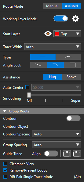
Step 28: Enable Working Layer Mode in the Add Connect widget.
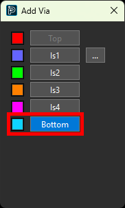
Step 29: Double-click to create a via. The Add Via window opens. Select Bottom to route on the bottom layer.
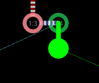
Step 30: A blind/buried via to layer 3 is created and a via to layer 4 is attached to your cursor at a fixed distance from the original via. Click to place the via and click to place additional vias until the bottom layer is reached.
Step 31: Press Escape to end routing.
Step 32: Click to start drawing a trace on the RA0 pad. Double-click to create a via and choose Bottom in the Add Via window.
Step 33: A stacked group of vias that spans the entire board is created.
Step 34: Click to place the stacked vias. Choose the Select mode from the toolbar to end connection mode.
Configuring Pad-Pad Constraints in OrCAD X
Step 1: Open the provided design in OrCAD X PCB Designer. OrCAD X includes a Constraints panel, allowing designers to define and assign constraint sets directly on the PCB canvas.
Step 2: Select Display > Windows > Constraints from the menu to open the Constraints panel if it is not already open.
Step 3: The Constraints panel opens on the right side of the canvas. This provides an efficient method for defining and assigning electrical, physical, and spacing constraints with the aid of a visual graphic. Scroll down to Physical to assign physical constraints such as pad-pad connection. Select Advanced to define all physical constraints available in OrCAD X.
Defining Pad-Pad Rules in OrCAD X
Step 4: Select the plus sign for Create Physical CSet to create a new CSet.
Step 5: The Create Spacing CSet window opens. Enter BB_STAGGER for the name.
Step 6: Click OK. The constraint set is automatically selected in the Rule Set dropdown.
Step 7: The bottom of the Physical subpanel shows a list of vias that can be placed in the constraint set. Select Edit Via List Dialog to modify the list.
Step 8: By default, all blind and buried vias and the default via can be placed. To remove the default via, double-click it in the Via List.
Step 9: Click OK to save the settings and close the window. The default through-hole via is no longer listed in the Via List.
Step 10: Set the BB Via Stagger minimum to 5 and maximum to 100.
Step 11: Select NOT_ALLOWED from the Pad-Pad Direct Connect menu. This will prevent any direct pad-to-pad connections on the nets with this constraint set.
Step 12: To create a rule set for stacked vias, select Create Physical CSet near the top of the subpanel again.
Step 13: Name the set BB_STACK and click OK.
Step 14: Set the minimum and maximum BB Via Stagger to 0.
Step 15: Select VIAS_VIAS_ONLY from the Pad-Pad Direct Connect dropdown. This will allow pad-to-pad connections only between vias.
Assigning Pad-Pad Rules to Nets in OrCAD X
Step 16: Constraint sets can be assigned to groups of nets in the Constraint Manager. Select Setup > Constraints from the menu to activate the Constraint Manager.
Step 17: The Constraint Manager window opens, showing a directory of constraint domains and worksheets. Select the Physical domain and the Net > All Layers worksheet.
Step 18: Select the cell under Referenced Physical CSet for net group A_GROUP. Select BB_STAGGER from the dropdown. The stagger constraint set is assigned to all nets in the group.
Step 19: Select the cell under Referenced Physical CSet for net group RA_GROUP and assign the BB_STACK constraint set to the group.
Step 20: Select Analyze > Analysis Mode from the Constraint Manager menu.
Step 21: The Analysis Modes window opens. Here you can enable all design rule checks available in OrCAD X. Select Physical from the list on the left.
Step 22: Select On for Pad-Pad Direct Connect to enable rule checks for pad-pad connections.
Step 23: Click OK to save the settings and close the window.
Step 24: Close the Constraint Manager.
Verifying Adherence to Pad-Pad Rules in OrCAD X
Step 25: Zoom into the unrouted pins of nets A1 and RA0 on U10, indicated by ratsnest lines.
Step 26: Select Route > Connect from the menu.
Step 27: Select net A1 to start routing.
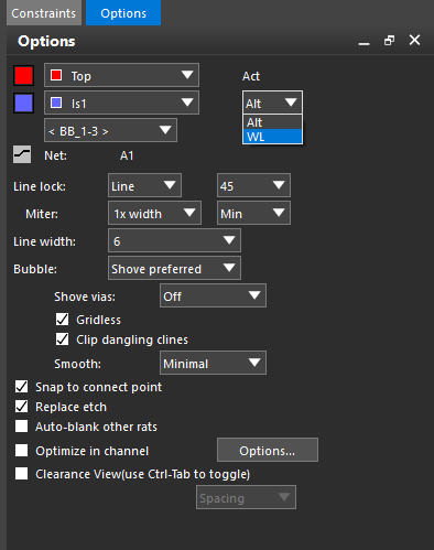
Step 28: Select WL from the dropdown in the Options panel.
Step 29: A window showing the active working layers opens. Leave the default settings and click Close.
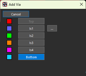
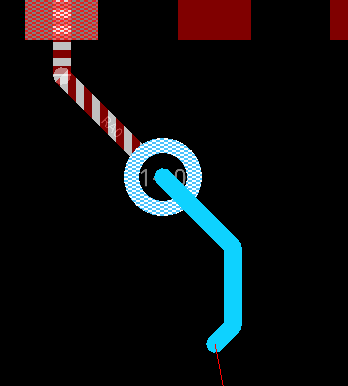
Step 30: Double-click to create a via. The Add Via window opens. Select Bottom to route on the bottom layer.
Step 31: A blind/buried via to layer 3 is created and a via to layer 4 is attached to your cursor at a fixed distance from the original via. Click to place the via and click to place additional vias until the bottom layer is reached.
Step 32: Right-click and select Next to end routing.
Step 33: Click to start drawing a trace on the RA0 pad. Double-click to create a via and choose Bottom in the Add Via window.
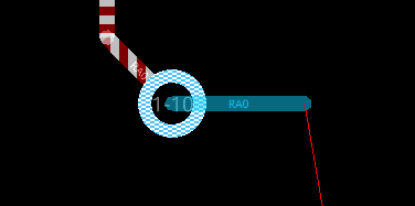
Step 34: A stacked group of vias that spans the entire board is created. Click to place the stacked vias. Right-click and select Done to place the trace and end routing mode.

