Stacked and staggered vias are crucial for boards containing high-density interconnect (HDI) devices. To improve signal integrity, provide routing flexibility, and increase the design density, vias can be placed on top of each other (stacked) or slightly offset (staggered) to accommodate manufacturer’s capabilities. Easily configure and use stacked or staggered vias in your high-speed PCB designs with Allegro PCB Designer.
This quick how-to will provide step-by-step instructions on how to create stacked vias with Allegro PCB Designer with the High-Speed Option enabled.
To follow along, use the provided design files above the table of contents.
How-To Video
Configuring a Staggered Via Structure
Step 1: Open the provided design, Viper_StackedVias.brd, with Allegro Venture or Allegro PCB Designer with the High-Speed Option enabled.
Step 2: From the menu, select Route > Connect or the Connect icon on the toolbar.
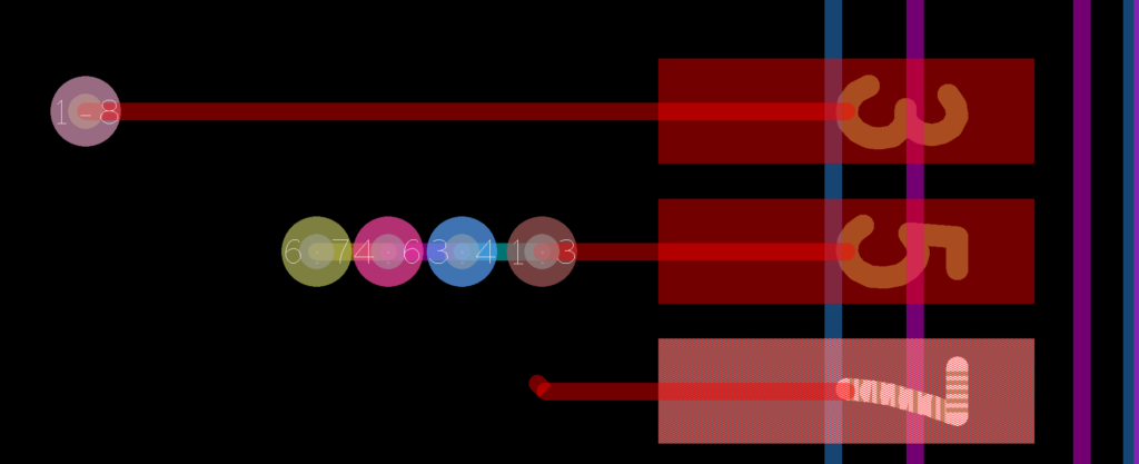
Step 3: Click to select pin 7 and begin routing.
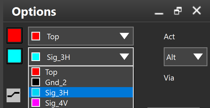
Step 4: In the Options tab, select Top as the starting layer and SIG_3H as the ending layer.
Step 5: Double-click the canvas to place the via.
Note: The active layer is automatically changed to SIG_3H in the Options tab.
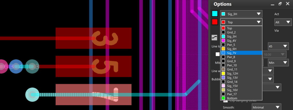
Step 6: In the Options tab, change the ending layer to Sig_7V.
Step 7: Double-click the canvas to place the via next to the existing via.
Note: Check with your board house to verify capabilities and the minimum distance required between stacked, offset vias.
Step 8: In the Options tab, change the ending layer to Gnd_11.
Step 9: Double-click the canvas to place the via next to the previously placed via.
Step 10: In the Options tab, change the ending layer to Sig_16V
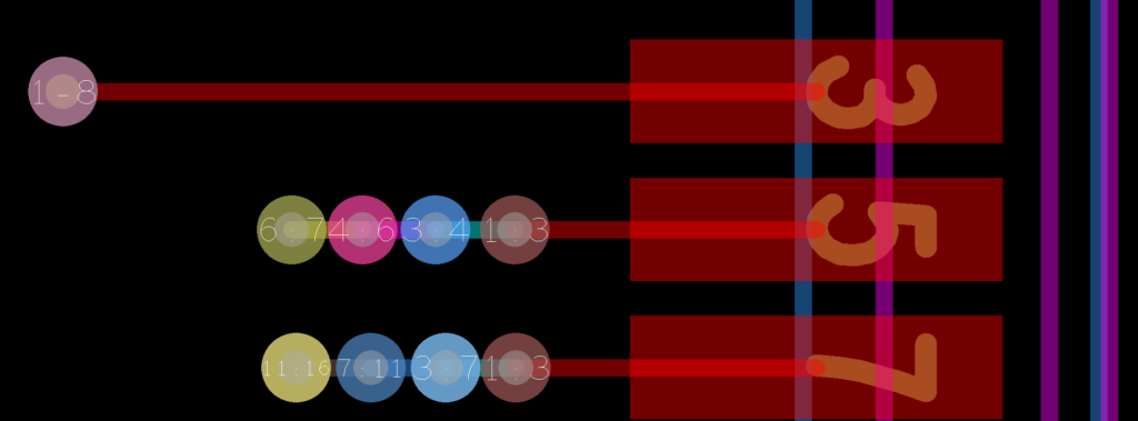
Step 11: Double-click the canvas to place the via next to the previously placed via.
Step 12: Right-click and select Done.
Creating a Staggered Via Structure
Step 13: From the menu, select Route > Structure > Create.
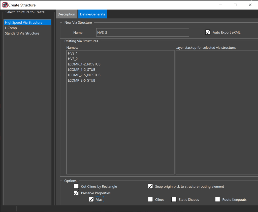
Step 14: In the Create Structure window, select Vias under Preserve Properties and leave all other defaults.
Step 15: In the PCB canvas, drag a box around the newly created via structure to select it.
Step 16: Give a name for the structure definition and click Save.
Note: The Via structure has been added to the Existing Via Structures list.
Step 17: Select OK or Enter on the keyboard to close the Create Structure window.
Placing a Staggered Via Structure
Step 18: From the menu, select Route > Structure > Place.
Step 19: In the Place Structure window, select the newly created via structure from the list and check Include Unassigned pins.
Note: For this example, selecting Include unassigned pins is required as this design does not have nets defined.
Step 20: Move the cursor to the PCB canvas.
Note: The via structure is attached to the cursor and ready to be placed in the design.
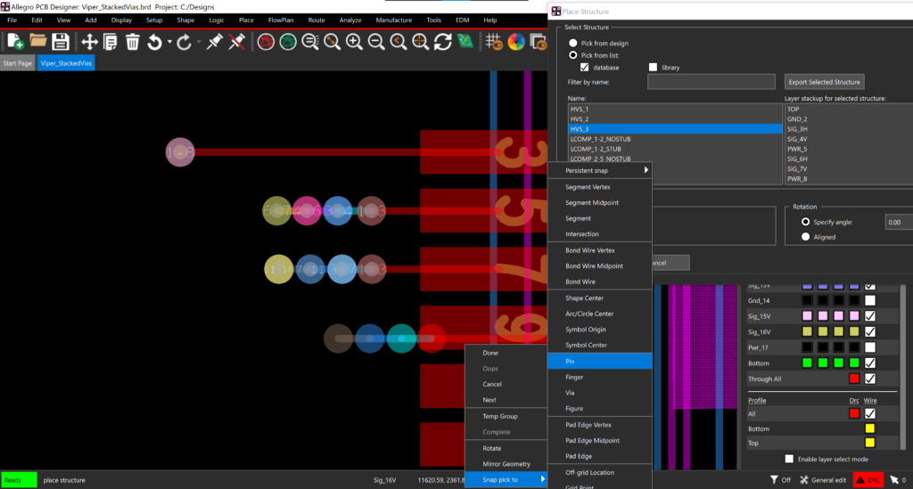
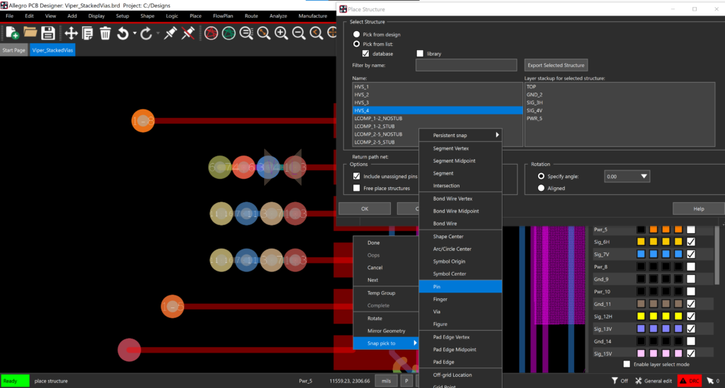
Step 21: Hover the cursor over pin 9. Right-click and select Snap pick to > Pin.
Step 22: Right-click and select Done.
Note: The Place Structure window is automatically closed.
Configuring a Stacked Via Structure
Note: Check with your manufacturer’s regarding their capabilities for stacked and staggered vias. Only some manufacturers are capable of producing designs with stacked vias.
Step 23: From the menu, select Route > Connect or the Connect icon on the toolbar.
Step 24: Click to select pin 11 and begin routing.
Step 25: In the Options tab, select Top as the starting layer and GND_2 as the ending layer.
Step 26: Double-click the canvas to place the via.
Step 27: In the Options tab, change the ending layer to Sig_3H.
Step 28: Right-click on the previously placed via and select Add Via.
Step 29: In the Options tab, change the ending layer to Sig_4V.
Step 30: Right-click on the previously placed via and select Add Via.
Step 31: In the Options tab, change the ending layer to PWR_5.
Step 32: Right-click on the previously placed via and select Add Via.
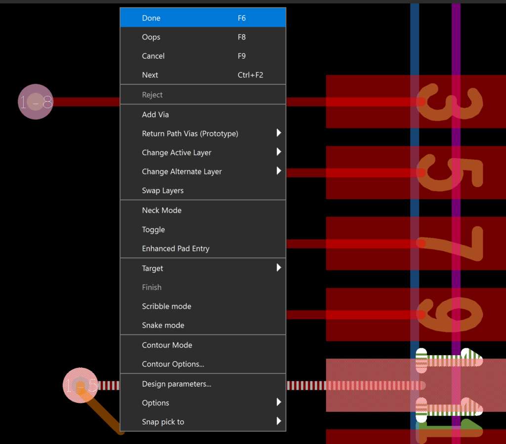
Step 33: Right-click and select Done.
Creating a Stacked Via Structure
Step 34: From the menu, select Route > Structure > Create.
Step 35: In the Create Structure window, select Vias under Preserve Properties and leave all other defaults.
Step 36: In the PCB canvas, drag a box around the newly created via structure to select it.
Step 37: Give a name for the structure definition and click Save.
Note: The Via structure has been added to the Existing Via Structures list.
Step 38: Select OK or Enter on the keyboard to close the Create Structure window.
Placing a Stacked Via Structure
Step 39: From the menu, select Route > Structure > Place.
Step 40: In the Place Structure window, select the newly created via structure from the list and check Include Unassigned pins.
Note: For this example, selecting Include unassigned pins is required as this design does not have nets defined.
Step 41: Hover the cursor over pin 13. Right-click and select Snap Pick To > Pin.
Step 42: Right-click and select Done.
Note: The Place Structure window is automatically closed.
Wrap Up & Next Steps
Easily use stacked or staggered vias in your PCB designs to improve signal integrity and increase routing flexibility with the advanced functionality of Allegro PCB Designer.

