When designing a high-speed PCB, delay is one of the most important aspects to consider. Even the smallest mismatch (in picoseconds) can be enough to cause high-speed nets to fail. With OrCAD, engineers can incorporate Z-axis delay and pin delay to ensure the accuracy of length matching for high-speed nets.
Z-axis delay incorporates the thickness of the PCB into the delay calculations. This takes the length when going through a via or a pin into consideration when calculating:
- Differential pairs
- Static or Dynamic phase
- Match groups such as minimum/maximum propagation delay
Pin Delay incorporates the distance from the die to the pin when calculating propagation delay. This value, in length or in time, can be sourced from the chip manufacturer.
This quick how-to will provide step-by-step instructions on how to incorporate pin delay and Z-axis delay in OrCAD PCB Designer.
How-To Video
Importing Delay Values
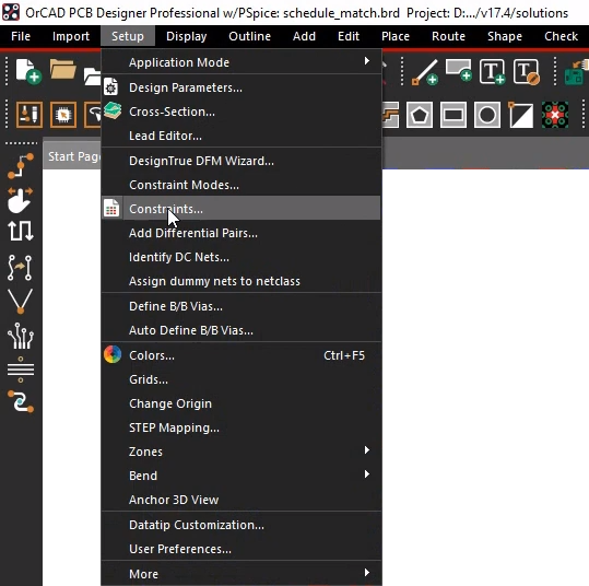
Step 1: Select Setup > Constraints from the menu.
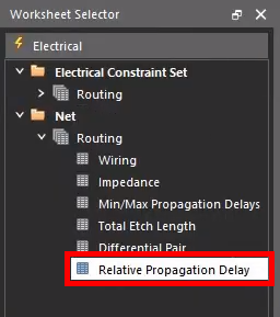
Step 2: From the Worksheet Selector, select the Electrical domain and the Net > Routing > Relative Propagation Delay worksheet.
Step 3: Right-click the desired match group and select Analyze.
Note: This will evaluate the existing propagation delay constraints. Constraints are analyzed against the values in the design.
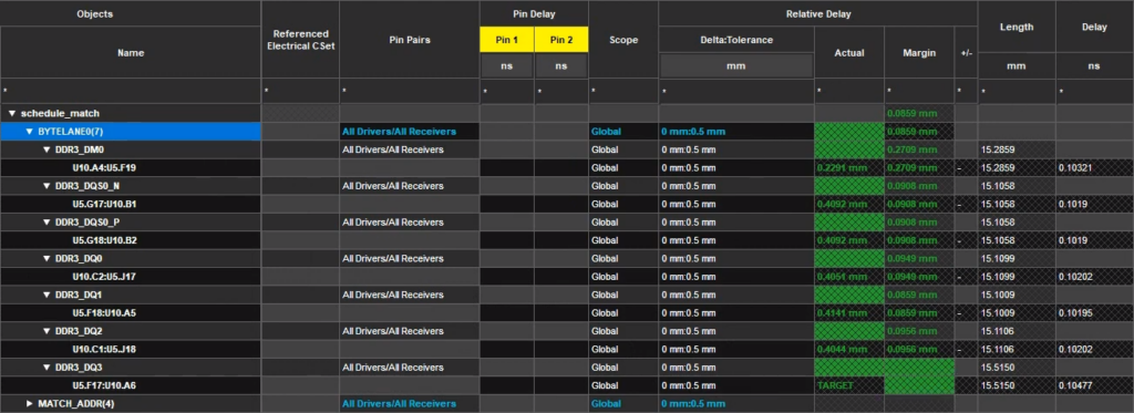
Step 4: Expand each net. Ensure that all Relative Delay values are green, indicating passing. Close the Constraint Manager.
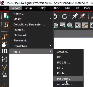
Step 5: Select Import > More > Pin Delay from the menu. The Pin Delay Import window opens.
Step 6: Select the ellipses to browse for the desired file.
Step 7: Select the desired pin delay file and click Open.
Note: This file browser defaults to search for CSV files. To load a text file, change the File of Type dropdown to All Files.
Step 8: Select Import to load the pin delay constraints and Close.
Note: This imports the pin delay values and applies the constraints to the chip automatically.
Enabling Delay Checks
Step 9: Select Setup > Constraints from the menu.
Step 10: Select the Electrical domain and the Net > Routing > Relative Propagation Delay worksheet.
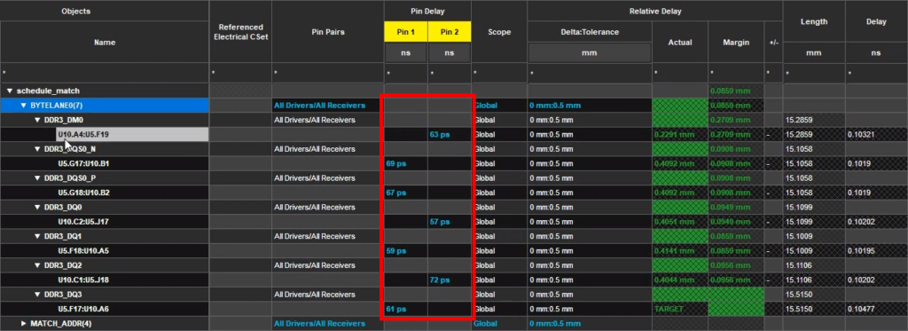
Step 11: Right-click the desired match group and select Analyze. The pin delay values have been imported.
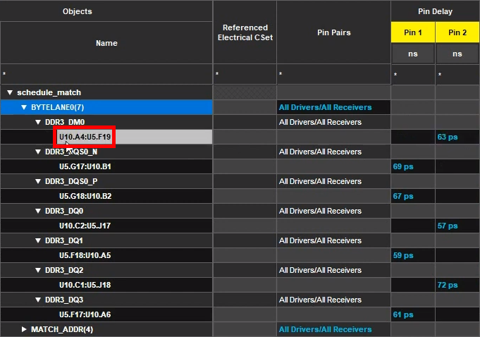
Note: Whether a delay value is defined under the Pin 1 or Pin 2 column depends on the direction of the trace.
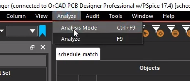
Step 12: To enable analysis of pin delay constraints, select Analyze > Analysis Modes from the menu.
Step 13: Select Electrical from the sidebar.
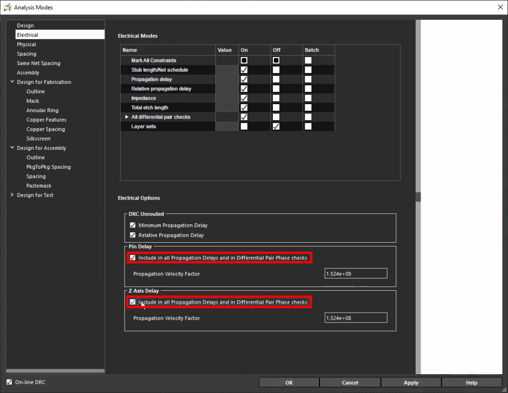
Step 14: Under Pin Delay, select the option to Include in all Propagation Delays and in Differential Pair Phase checks to enable the constraints.
Step 15: Enable the same option under Z-Axis Delay.
Note: Adjust the Propagation Velocity Factor for the Pin Delay and Z-Axis Delay if required.
Step 16: Click Apply and OK to save the settings and close the window.
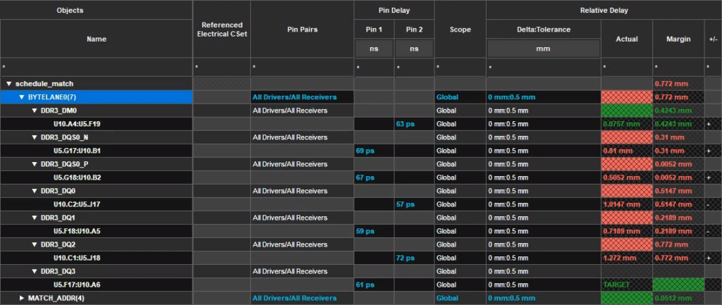
Step 17: View the relative delay results again.
Note: Failing length-matching values, due to the Z-axis and pin distances, are highlighted in red.
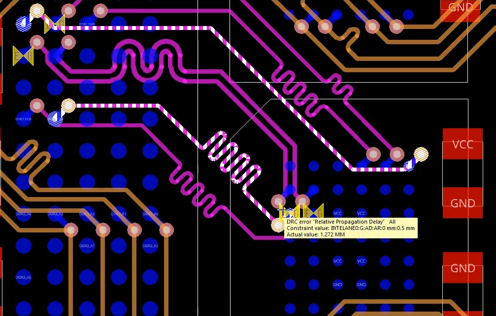
Step 18: Minimize the Constraint Manager and view the DRCs on the board. Hover your cursor over an error for more information.
Note: Errors can be corrected by adding or removing delay, depending on the type of error.
Correcting Delay Errors
Step 19: To remove delay, select Route > Slide from the menu or the Slide button from the toolbar.
Step 20: Select the edge of a delay tuning to slide it. Click again to drop the edge.
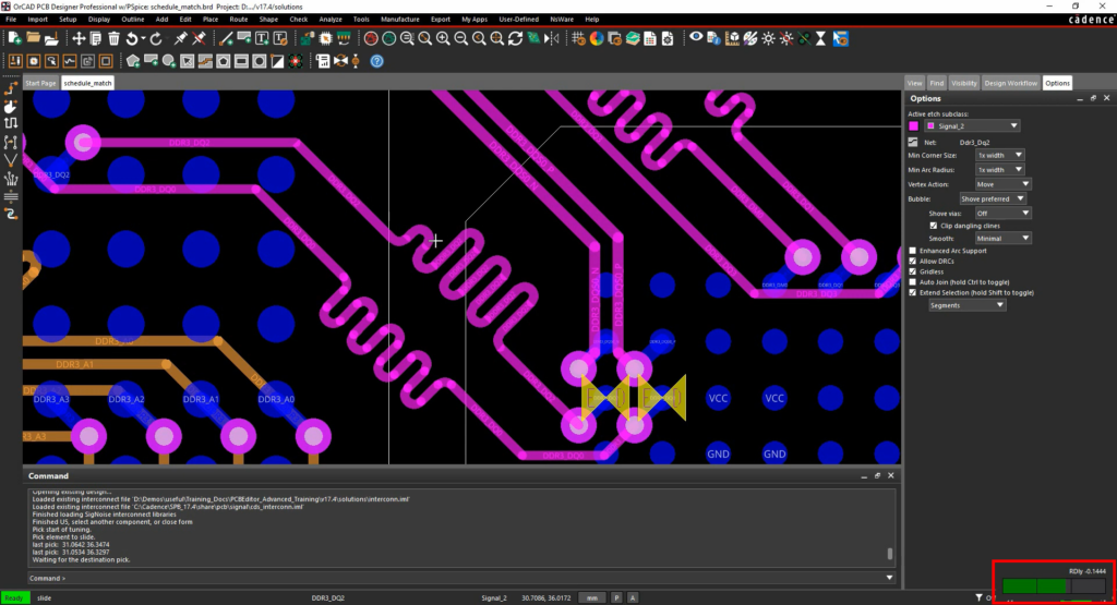
Note: Pay attention to the heads-up display in the bottom-right of the screen. This timing meter provides real-time feedback to help meet the required constraints. When the bar turns green, the relative delay constraints are met.
Learn how to detach the timing meter and have this real-time feedback attached to your cursor here.
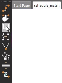
Step 21: To add delay, select Route > Delay Tuning from the menu or the Delay Tuning button from the toolbar.

Step 22: Configure the tuning style, gap, corners, and etch layer in the Options panel.
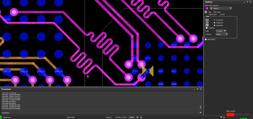
Step 23: Select the desired trace to add the delay.
Note: Pay attention to the timing meter to efficiently adhere to the required delay. You can similarly remove existing delays by selecting it with the Delay Tuning tool active.
Step 24: When all DRCs are cleared, return to the Constraint Manager. Right-click in the worksheet table and select Analyze.
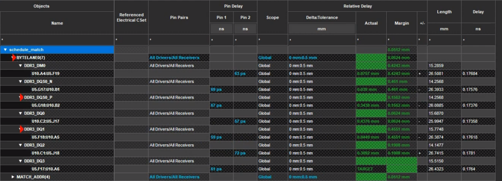
Step 25: View the results. All Relative Delay values are green, indicating that all errors are cleared.
Wrap Up & Next Steps
Ensure the accuracy of high-speed nets by incorporating pin delay and z-axis delay into length matching calculations with the advanced capabilities of OrCAD PCB Designer Professional. Test out this functionality and more with a free trial of OrCAD.

