During the design review process, it’s critical to examine all aspects of the PCB design before production to ensure functionality, manufacturability, and accuracy of the PCB design and documentation. A standard review of generated artwork, PDFs, and accompanying documentation often doesn’t provide enough information for a comprehensive evaluation and tying up a software license just to review a board is not an optimal choice. With the OrCAD/Allegro PCB Free Viewer, stakeholders can intelligently review the PCB design, easily accessing the design database and important design information. By using the OrCAD/Allegro PCB Free Viewer, teams can:
- Improve communication
- Reduce errors
- Increase efficiency
- Free-up licenses for design work
- Streamline the design review process
This quick how-to will provide step-by-step instructions on how to use the OrCAD/Allegro PCB Free Viewer to streamline the design review process.
To follow along, download the provided files above the table of contents.
How-To Video
Opening a Design with the PCB Free Viewer
Step 1: Open the OrCAD/Allegro PCB Free Viewer.
Note: For new OrCAD/Allegro PCB Free Viewer users, download the software here.
For users with full versions of OrCAD or Allegro installed, open the OrCAD/Allegro PCB Free Viewer using the executable file, allegro_free_viewer.exe, found here:
- For Version 17.4: C:\Cadence\SPB_17.4\tools\bin
- For Version 22.1: C:\Cadence\SPB_22.1\tools\bin
If you are using version 22.1 on a high-definition monitor, easily scale the OrCAD/Allegro PCB Free Viewer using these instructions.
Step 2: Select File > Open from the menu.
Step 3: Select the provide design, pcbtutorial.brd, from the downloaded materials and click Open.
Configuring Visibility
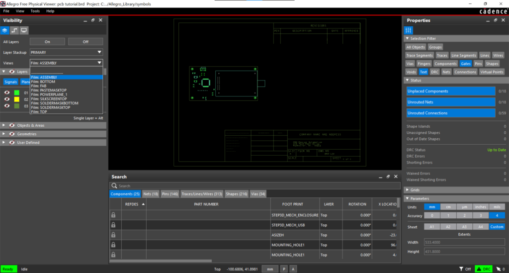
Step 4: In the Visibility tab, under Views, select Films: ASSEMBLY from the drop-down selection to view the assembly drawing.
Note: If this tab is not visible select View > Visibility from the menu. Views are pre-populated based on the Gerber artwork setup and generation.
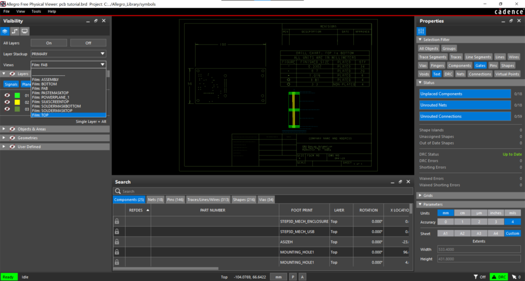
Step 5: Select the drop-down menu under Views again and choose FILMS: FAB to view the fabrication drawing.
Step 6: Under Views, select Film: TOP from the drop-down menu.
Step 7: Select the On button to turn all layers of the PCB design on.
Note: Select the Off button to turn all layers of the PCB off.
Step 8: Click the arrow next to Layers to expand the layers in the design.
Note: This view allows you to customize the visibility shown in the PCB canvas.
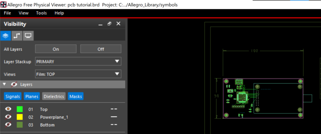
Step 9: Click the eye icon next to the Powerplane_1 and Bottom layers to turn visibility off.
Step 10: Click the arrow next to Objects & Areas to expand the objects in the design.
Step 11: Define your selection by clicking the desired objects and areas.
Note: Visibility for the following objects and areas can be adjusted:
- Signals
- Planes
- Dielectrics
- Masks
- Pins
- Vias
- Traces
- Shapes
- Text
- DRC
- Via Keepout
- Route Keepout
- Package Keepout
- Regions
Step 12: Click the arrow next to Objects & Areas again to contract the category.
Step 13: Click the arrow next to User Defined to expand the User-defined classes and subclasses in the design.
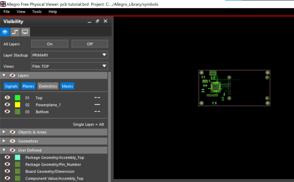
Step 14: Select the eye icon next to User Defined to turn the visibility off for all items in the user defined category.
Step 15: Select the arrow next to User Defined again to contract the category.
Modifying the PCB Canvas View
Step 16: Use the arrow keys on the keyboard to move the view on the PCB canvas.
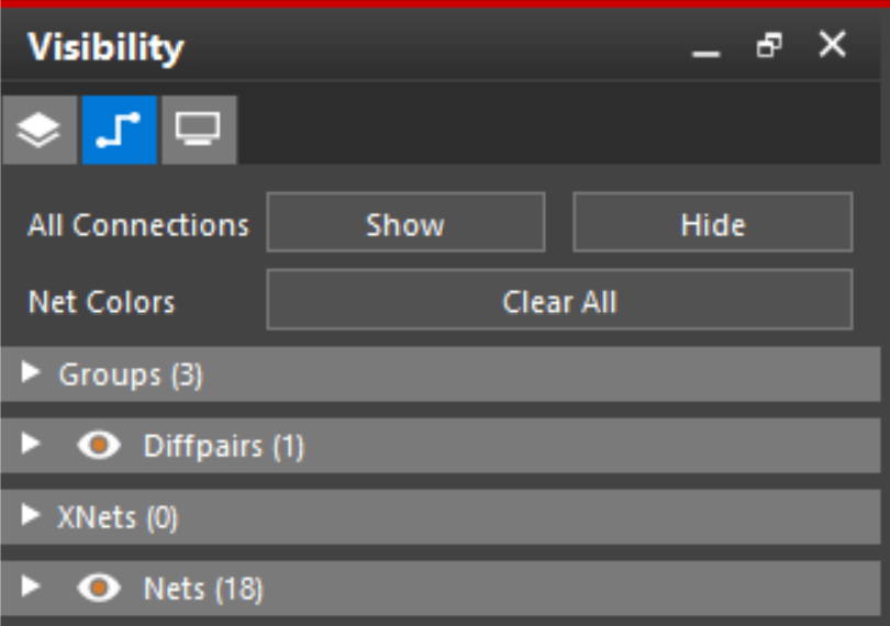
Step 17: In the visibility tab, select the Net tab.
Note: Here you can configure visibility for:
- Nets
- Net groups
- Differential pairs
- Xnets
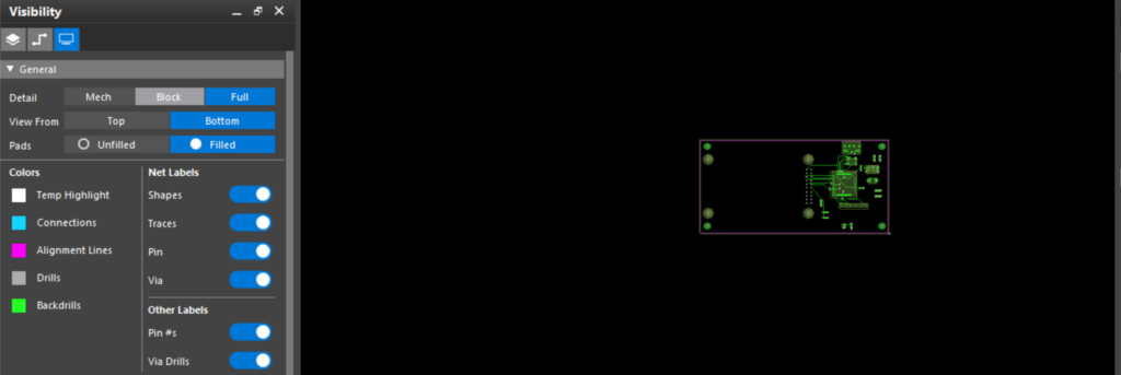
Step 18: In the Visibility tab, select the General tab.
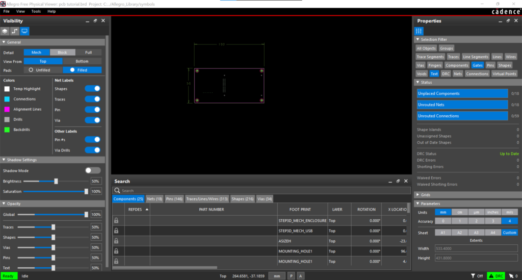
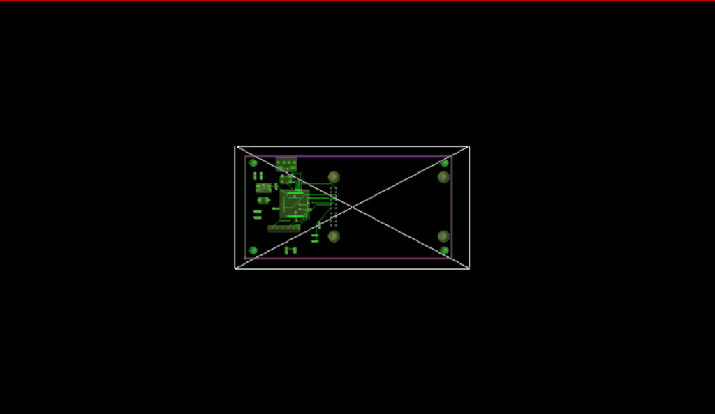
Step 19: Under Detail, select Mech.
Note: This will display only the mechanical elements in the design.
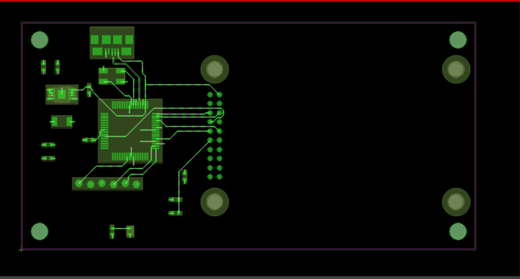
Step 20: Under Detail, select Full.
Note: This will display the full design on the PCB canvas.
Step 21: Under View From, select Bottom.
Note: This will display the bottom side of the board.
Step 22: Under View From, select Top.
Step 23: Under Opacity, adjust the scale for Global opacity.
Note: Opacity can also be controlled individually for traces, shapes, vias, pins, and text.
Step 24: In the menu, select View > Zoom Points.
Step 25: Click the canvas. Move the cursor to draw a box around the desired view. Click again to complete the box.
Note: Other zoom options are available to configure the view on the PCB canvas including:
- Zoom In
- Zoom Out
- Zoom Fit: Zooms to the extent of the board.
- Zoom World: Reduces the magnification of your design so you can view your entire drawing.
- Zoom Center: Moves the indicated point in the drawing into the center of the window display.
- Zoom Previous: Zooms from the current window extents to the prior view.
Viewing Design Properties
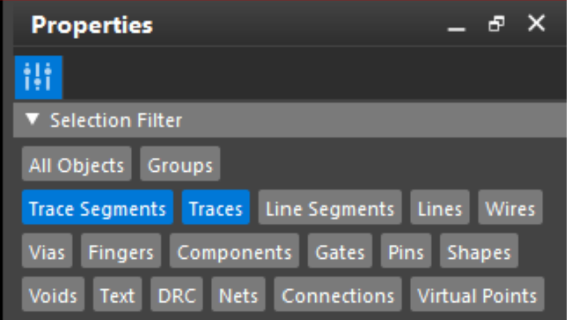
Step 26: In the Properties tab, under Selection Filter, choose the desired objects to be selected in the PCB. Ensure Trace and Trace Segments are selected.
Note: Click the corresponding button to select or deselect an object.
Step 27: Make a selection in the PCB canvas by clicking and dragging the mouse.
Note: Only the traces and trace segments in the design have been selected.
Step 28: Click an open area in the PCB canvas to deselect the traces and trace segments.
Step 29: In the Selection Filter, select All Objects to select all items in the PCB design.
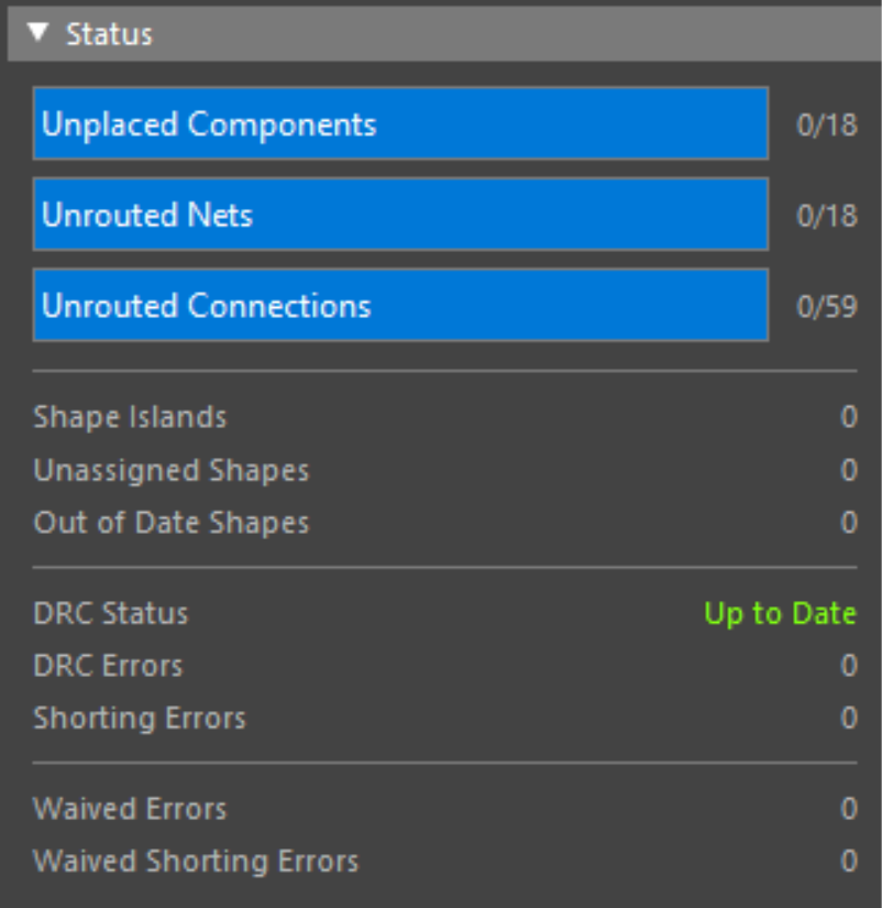
Step 30: View the Status of the design.
Note: Here users can review the number of unplaced components, unrouted nets, and unrouted connections as well as review information on any Design Rule Check (DRC) errors.
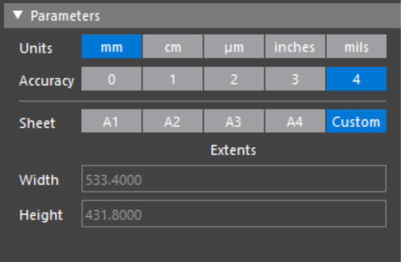
Step 31: View the Parameters used for the design.
Note: Here users can review the units, accuracy, and sheet size used for the design to ensure accordance with the project specifications.
Searching the PCB Design
Step 32: In the Search Results tab, view the available search categories. Click a tab to view the corresponding items in the category.
Note: If this window is not activated, select View > Find from the menu. Search categories include:
- Components
- Nets
- Pins
- Traces/Lines/Wires
- Shapes
- Vias
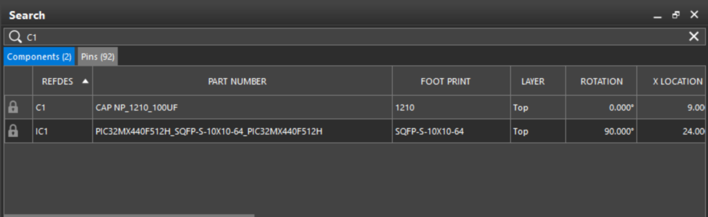
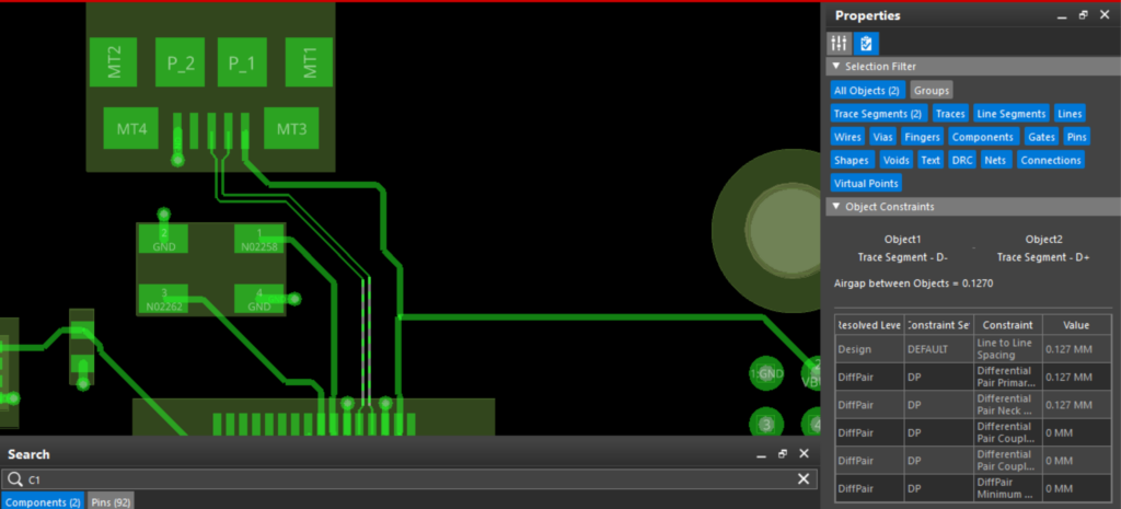
Step 33: In the Search Results tab, with Components selected, type C1 into the search bar. Press Enter.
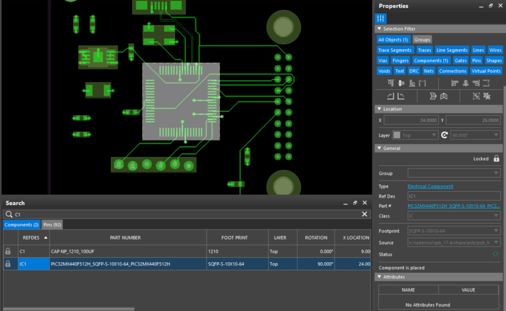
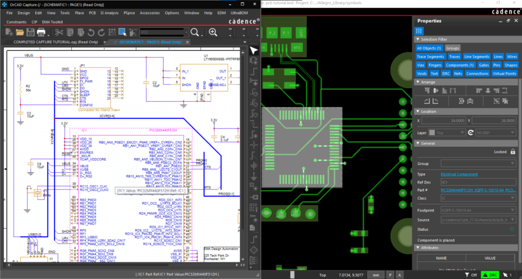
Step 34: Double-click IC1 from the search results.
Note: This will bring you to the location on the PCB canvas and provide additional information in the properties tab.
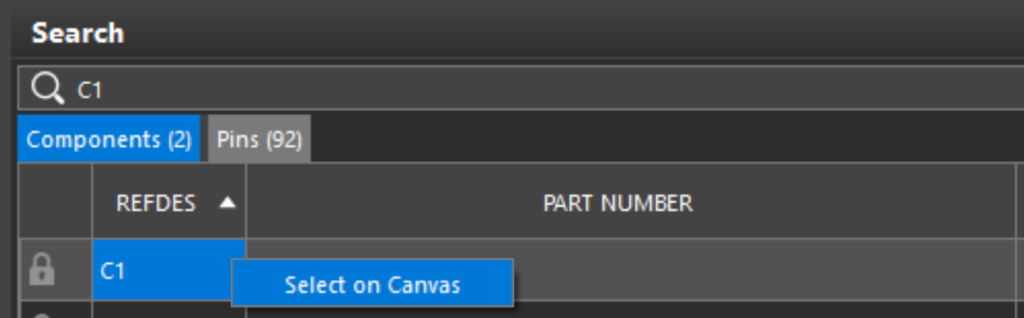
Step 35: In the search results, right-click on C1 and choose Select on Canvas.
Cross-Probing with a Schematic
Step 36: Open the corresponding schematic, complete capture tutorial.dsn, from the downloaded materials in the OrCAD Capture Free Viewer.
Note: For more information on how to use the OrCAD Capture Free Viewer, check out this how-to.
Step 37: Select a component on the schematic.
Note: The view will zoom into the corresponding area on the PCB and the footprint will be selected for easy review. If needed, close the visibility panel to improve the PCB canvas view.
Step 38: Select a net or bus in the schematic to review the information in the PCB canvas.
Step 39: Close the OrCAD Capture Free Viewer.
Reviewing Measurements
Step 40: Return to the OrCAD/Allegro PCB Free Viewer. Hold down ALT on the keyboard and select the mounting hole in the upper left corner of the PCB.
Note: Remember to set the selection filter to the desired configuration.
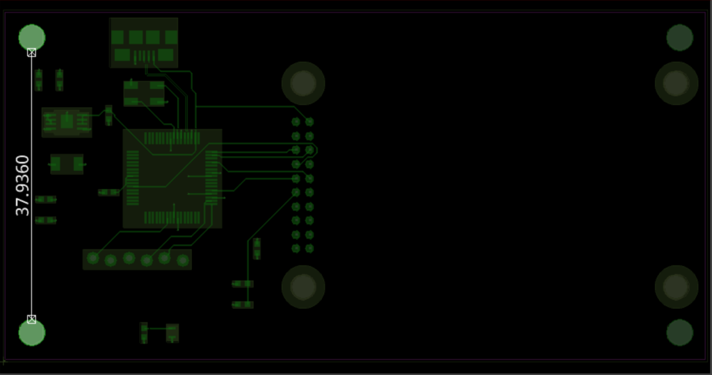
Step 41: With the ALT key still pressed, hover over the mounting hole in the bottom left corner of the PCB.
Note: Dynamic measurement will be displayed directly on the PCB canvas.
Step 42: Move the cursor to measure the distance between the mounting hole and X1. View the measured distance.
Step 43: Move the cursor to measure the distance between the mounting hole and the edge of the board. View the measured distance.
Step 44: Release ALT when measurements are finished.
Reviewing Design Details
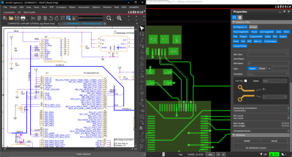
Step 45: Select the differential pair nets between IC1 and X1 on the PCB canvas.
Step 46: In the Properties Panel, select the Constraint tab.
Step 47: View the associated rules or constraints for the nets. Click an open space in the PCB canvas to deselect the nets.
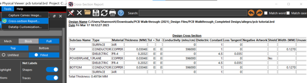
Step 48: Select Tools > Cross-section Report from the menu.
Note: This will activate a new window displaying detailed information about the board stack up.
Step 49: Close the Cross-section report.
Reviewing a Design in 3D
Step 50: Select View > 3D Canvas from the menu.
Step 51: Configure the 3D Canvas Filter for the desired visibility and click OK.
Step 52: In the 3D Canvas, select the Symbols tab.
Note: If the Symbols tab is not visible, select View > Windows > Symbols from the menu.
Step 53: Select the arrow next to TOP to display all the components and models in the design.
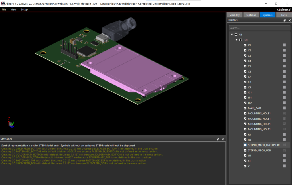
Step 54: Select the box next to STEP3D_MECH_ENCLOSURE to turn visibility off for the mechanical housing.
Step 55: Select the Nets tab.
Note: If the Nets tab is not visible, select View > Windows > Nets from the menu.
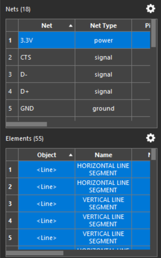
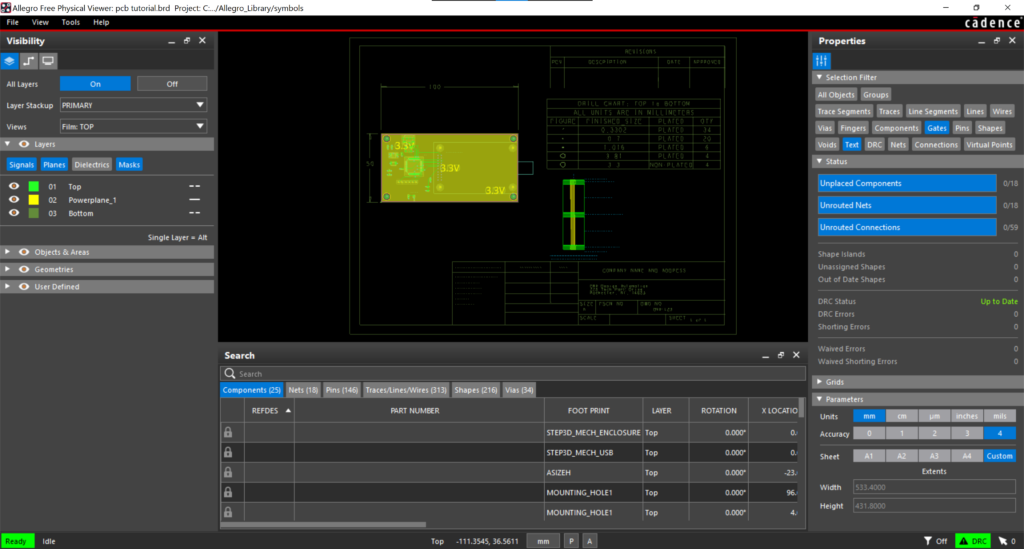
Step 56: Select net 3.3V. View the Net information.
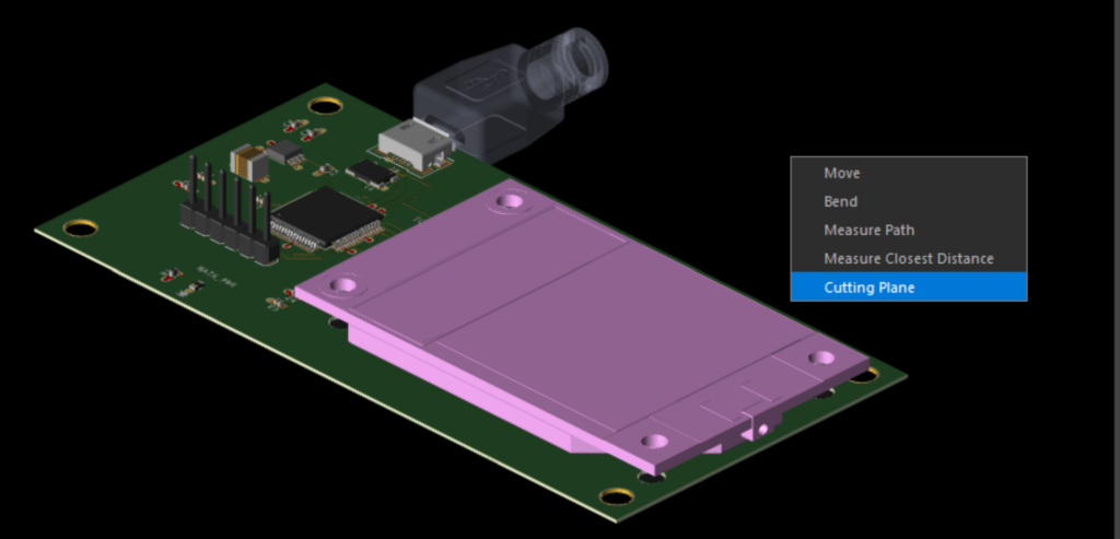
Step 57: Right-click the 3D Canvas and select Cutting Plane.
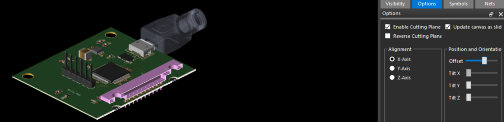
Step 58: Ensure Enable Cutting Plane and X-Axis are selected. Move the scale for the Offset to adjust the cutting plane of the design for a comprehensive analysis.
Step 59: Close the 3D Canvas.
Reporting with the Cadence PCB Editor Viewer
Step 60: From the menu, select Tools > Capture Canvas Image.
Note: This will take a screenshot of the current view in the PCB canvas which can be saved as an image.
Step 61: Add a name for the image, browse to the desired location, and click Save.
Step 62: To generate a PDF, select File > Print.
Step 63: Ensure the Name is set to Microsoft Print to PDF and click OK.
Step 64: Add a name for the PDF export, browse to the desired location, and click Save.
Wrap Up & Next Steps
Streamline design reviews, improve communication, and reduce errors by utilizing the OrCAD/Allegro PCB Free Viewer. Download your copy of the OrCAD/Allegro Free Viewer here to get started.

