To accelerate fabrication and decrease costs, PCBs are manufactured on panels; however, these panels have a direct effect on manufacturing costs. The more panels required to produce the desired quantity of PCBs, the higher the cost of manufacturing. To reduce the number of panels required, ensure space is used efficiently in the panel layout. Optimize your manufacturing panels with the Fab Panelization Tool in OrCAD PCB Designer Professional. Using Panelization you can improve the panel layout, ultimately reducing the number of panels and decreasing your manufacturing costs with features such as:
- Mirroring
- Board rotation
- Automatic array creation
- Family panel support
This how-to will provide step-by-step instructions on how to use Panelization in OrCAD PCB Designer Professional to optimize manufacturing panels.
To follow along, download the design files provided above the table of contents.
How-To Video
Designing Manufacturing Panels
Step 1: Open a blank panel (panel_start.brd) in OrCAD PCB Designer Professional.
Note: This and other examples can be found in the Cadence directory: C:\Cadence\SPB_17.4\share\pcb\toolbox\getting_started\panelization\pcb_context
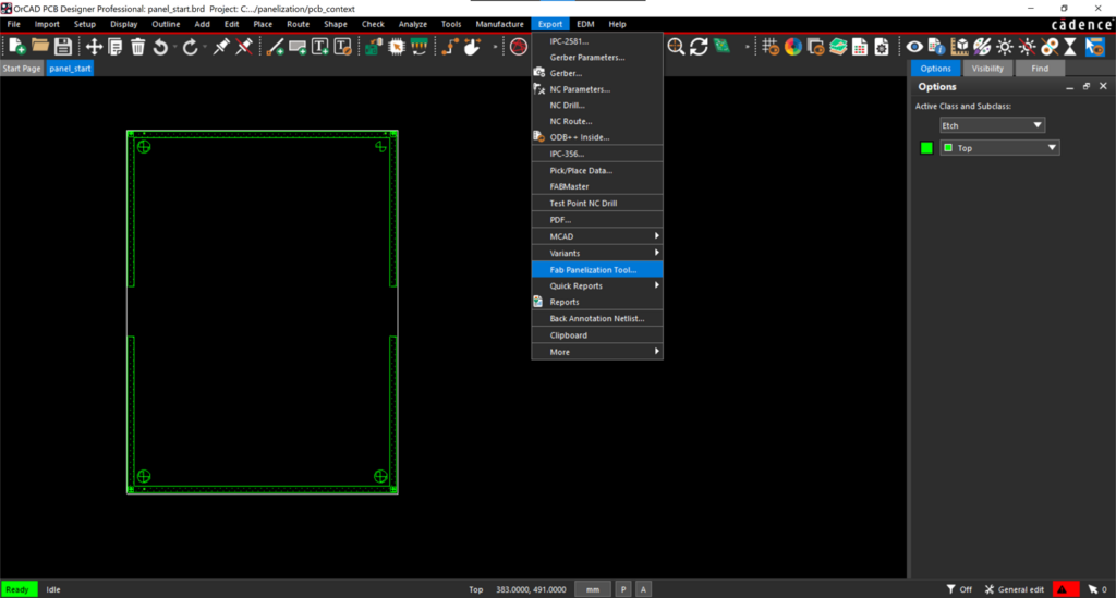
Step 2: Select Export > Fab Panelization Tool from the menu.
Note: The Fab Panelization Tool will not work on boards that are linked to logic (schematic) or netlisted; always begin with a new panel.
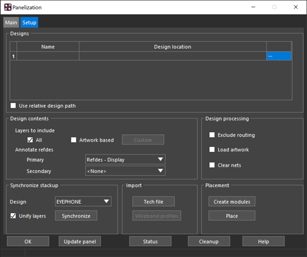
Step 3: Select the Setup tab in the Panelization window. Select the ellipses and browse for the location of the desired PCB.
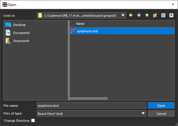
Step 4: Select the design and click Open.
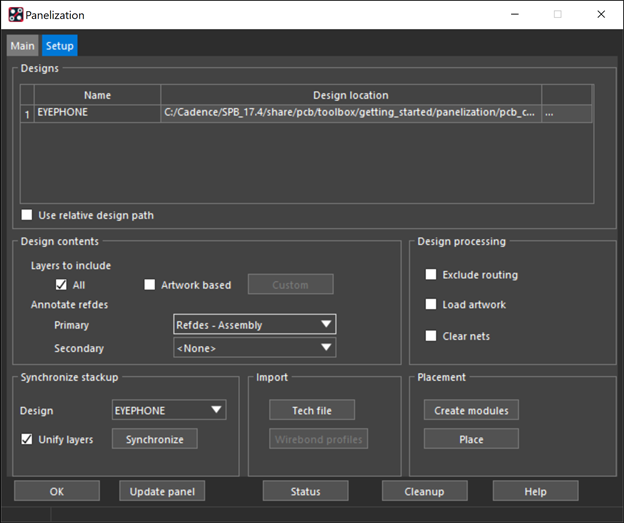
Step 5: Under Layers to Include, select All. Select Refdes- Assembly under Annotate Refdes: Primary.
Note: Layers to include controls the data read from the database into the panel. By selecting All, all layers will be visible in the module. If selecting Artwork, all layers from the artwork definitions (film setup) will be visible in the module. Setting the Primary Annotation to Refdes-Assembly will copy the original reference designators to the documentation subclasses: Package Geometry/PNL_Refdes_Assembly_Top and Package Geometry/PNL_Refdes_Assembly_Bottom.
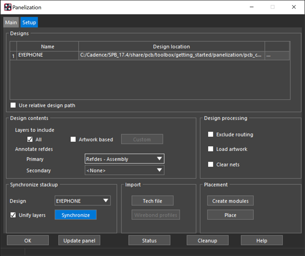
Step 6: Under Synchronize Stackup, select Unify layers and Synchronize.
Note: This function will adjust the stackup in the panel database to match the reference board.
Panel Layout
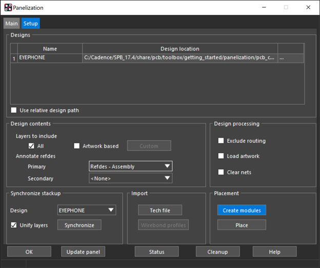
Step 7: Under Placement, select Create Modules.
Note: This will create a module of the board, including the size information and actual outline data required for interactive placement.
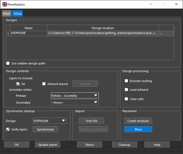
Step 8: Under Placement, select Place.
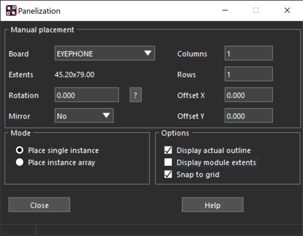
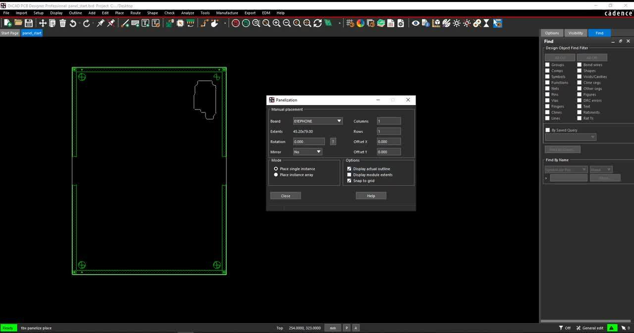
Step 9: Under Options, select Display actual outline.
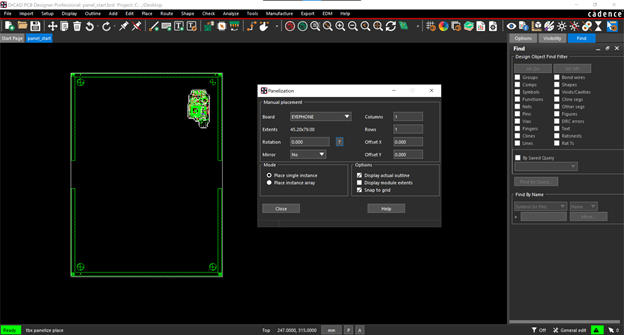
Step 10: Click the canvas to place the module.
Note: When placing a single instance, change the rotation and mirror settings to optimize the manufacturing panel. If a module was placed in error, select Close in the Panelization window.
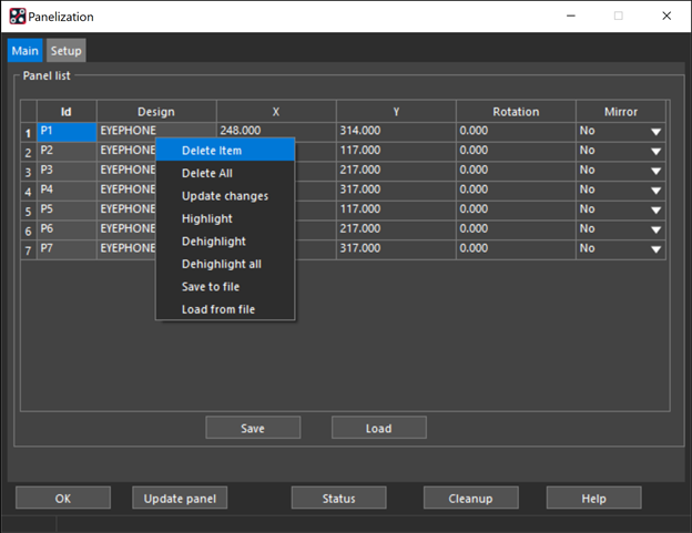
Select the Main tab in the Panelization window. Right click on the module and select Delete Item.
Panel Layout with Board Array
Step 11: Under Mode, select Place Module Array.
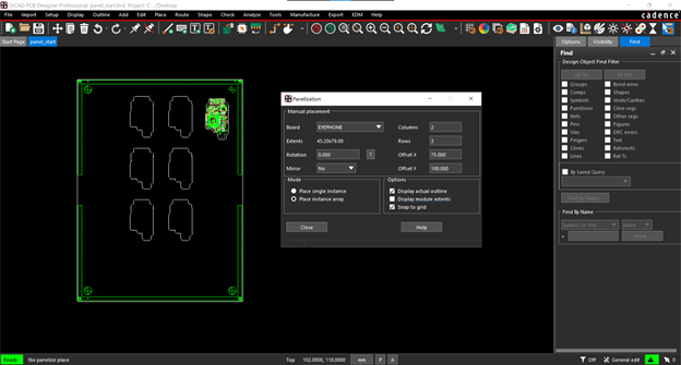
Step 12: Set the Column to 2, Rows to 3, Offset X to 75 and Offset Y to 100. Click to place on the panel.
Note: This will automatically setup an array of your design adhering to the defined specifications.
Step 13: Select Close.
Note: If you need to complete a family panel with multiple boards, select the Setup tab in the Panelization window. Right click and select Add Row. Complete the same process with the new design. The stackups must be the same for each board placed within the panel.
Step 14: Click OK to close the Panelization window.
Note: If a PCB design has been modified after placement in the fabrication panel, select Update Panel in the Panelization Window to automatically update the placed modules.
Wrap Up & Next Steps
Decrease the number of panels required for fabrication and consequently your manufacturing costs by optimizing the panel layout with the Fab Panelization tool in OrCAD PCB Designer Professional. To test out this functionality and optimize your design process, get your free trial of OrCAD.

