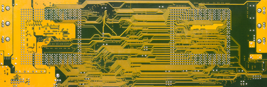
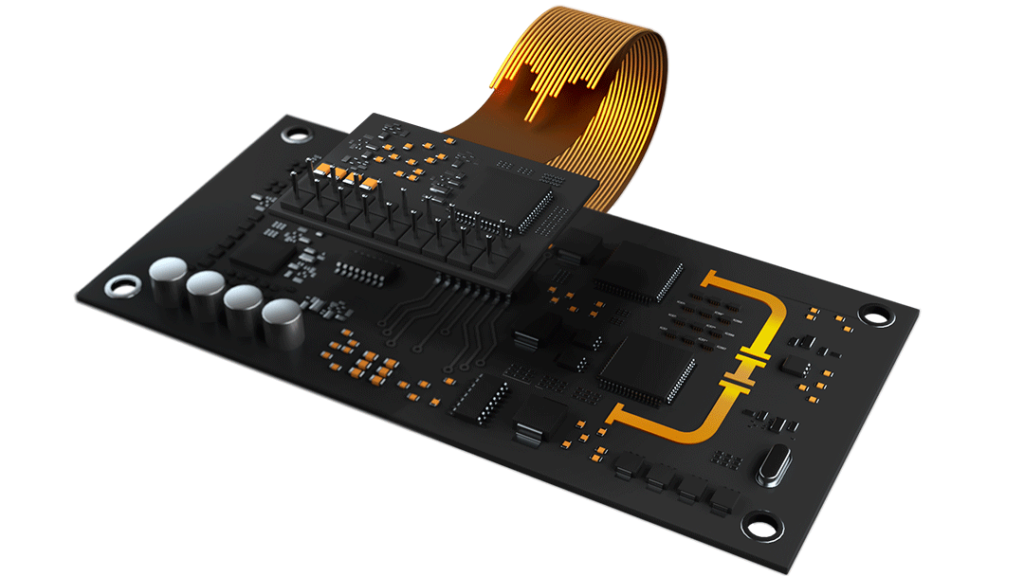
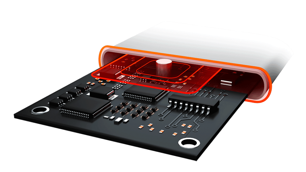
High-Density Interconnect (HDI) routing is a PCB design technique used to create boards with a high density of components and interconnections. HDI routing enables the placement of more components in a smaller area, making it popular for applications that demand compact, lightweight, and high-performance designs, such as smartphones, tablets, medical devices, and high-speed computing equipment. HDI routing utilizes a combination of microvias, blind and buried vias, laser-drilled vias, and sequential layers to create high-density, high-performance PCB layouts that are essential in modern electronic devices. HDI boards are more intricate, requiring careful planning to manage small trace widths, tight spacing, high via densities, and manufacturing complexities.
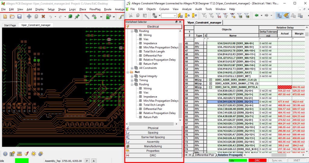
HDI boards require precision and accuracy to achieve a high-performance layout that can be successfully manufactured. OrCAD X and Allegro X include the necessary rules to configure your HDI routing including:
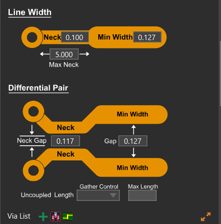
Via Stacking Constraints
Via to Pad Spacing Constraints
Same Net Spacing Constraints
With HDI rules configured, HDI routing can be efficiently completed in OrCAD X and Allegro X with:
Microvia Support
Blind and Buried Via Support
Layer Selection During Via Placement
Stacked and Staggered Via Support
Efficient Split Stack Selection
Guarantee the accuracy of your HDI routing and ensure a manufacturable board with the HDI constraints and routing functionality included in OrCAD X and Allegro X.
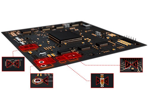
Key Features of HDI Routing in OrCAD X
OrCAD X and Allegro X contain the functionality you need to accurately and efficiently complete your HDI routing.
Via Stacking Constraints
Adhere to specific manufacturing rules for HDI routing and via stacking. Stack vias, defining how different types of vias can be stacked on top of each other including vias to pins, vias to vias, microvias to microvias only, and more.
Spacing Constraints
Configure and manage same net spacing rules for microvias to configure your HDI routing requirements. Define rules such as allowing microvias to touch or pads to overlap using negative numbers which will default spacing to the defined hole-to-hole constraint values.
Complex Via Support
OrCAD X and Allegro X support multiple via structures including microvias, blind vias, and buried vias allowing you to configure the required complex via structures for your HDI designs. Easily define the vias which should be used during routing using constraints for improved accuracy and reduced errors.
Pro
Via Layer Selection
Working layer mode allows you to select which layer you are routing to when placing vias. Easily select the desired layer in the pop up selection and the via required to transition layers is automatically selected.
Pro
Stacked and Staggered Vias
Easily create stacked via configurations and staggered via configurations to accommodate manufacturer’s capabilities, improve signal integrity, provide routing flexibility and increase the design density. Vias can be placed directly on top of each other (stacked) or slightly offset (staggered) based on rule definition.
Pro
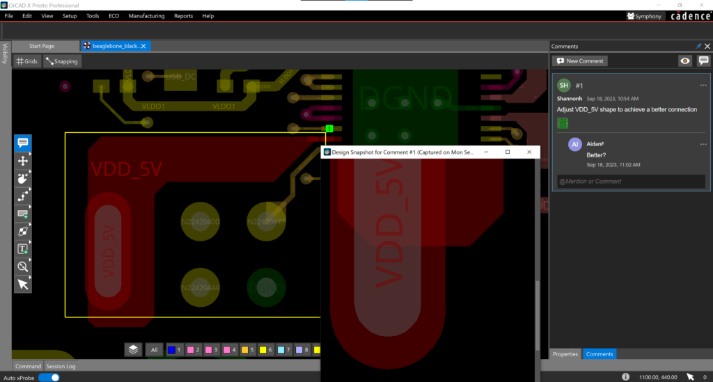
Split Stack Selection
Split via stacks that have already been placed with a cross-section view and easy selection of included vias to efficiently modify your HDI routing.
Get the PCB Design Capabilities You Need Today and Tomorrow
Let our team help you craft the perfect PCB design solution for your requirements. Contact us for more information.