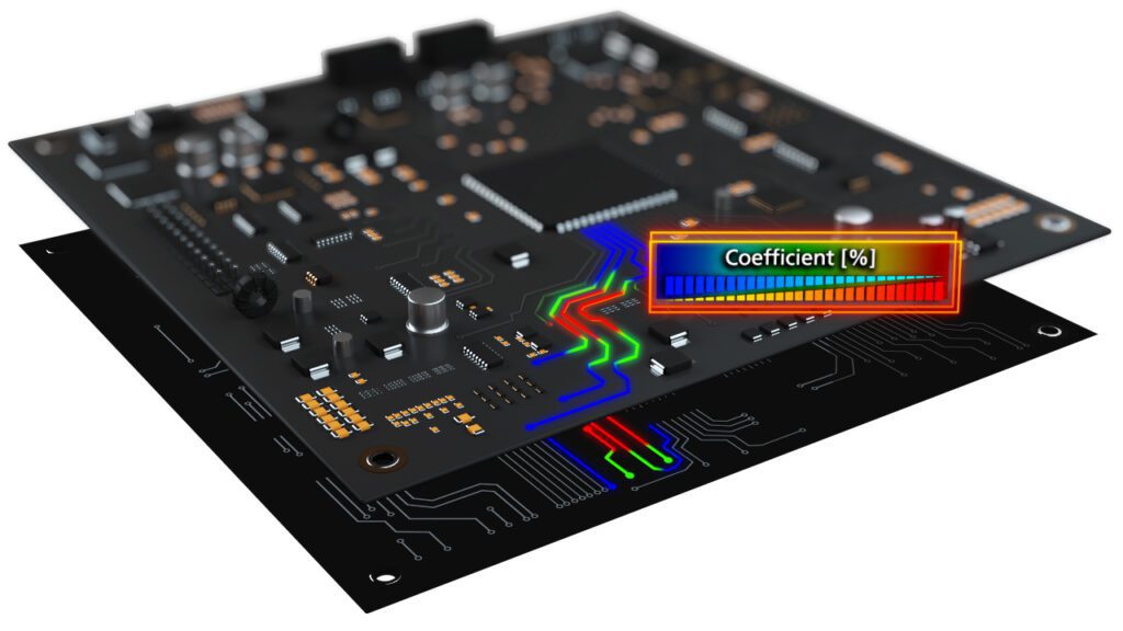
In today’s electronics landscape, product complexity is growing while time-to-market windows are shrinking. From signal and power integrity to EMI, thermal concerns, and beyond—modern PCB designs face interrelated electrical challenges that demand more than intuition and traditional testing can provide. To meet these evolving requirements, Multiphysics simulation is no longer optional, it’s essential.
In a recent webinar hosted by EMA Design Automation, experts Chris Banton and Matthew Harms broke down the key barriers to widespread simulation adoption and demonstrated how Cadence® Sigrity™ X addresses these head-on with a simulation-driven, AI-enhanced, analysis platform.
Why Traditional Simulation Falls Short
Many engineers still avoid simulation, despite knowing the benefits. When EMA asked engineers why, the answers were familiar:
- Setup is time consuming and complex
- Tool expertise is siloed with a few specialists
- Simulation coverage is limited, leading to partial insights
- Project timelines don’t allow room for traditional simulation overhead
- Cost models don’t align with occasional use
- And, “we haven’t had problems…..yet.”
Famous examples like Apple’s “Antennagate” and Microsoft’s “Red Ring of Death” remind us that simulation gaps can result in costly redesigns, recalls, and reputation damage. Forward-thinking organizations are now integrating simulation early and often to ensure functionality and foster innovation.
Enter Sigrity X: Simulation Reimagined
To meet these needs, Sigrity X offers a rearchitected approach to PCB simulation:
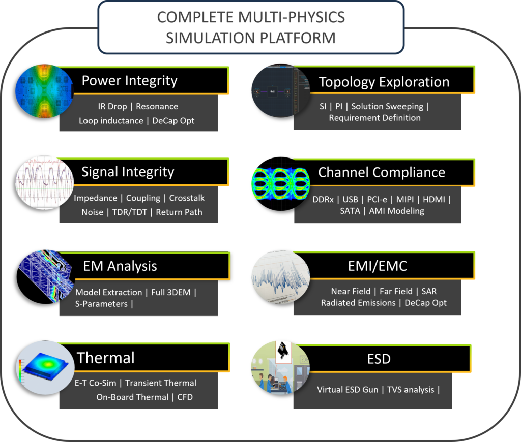
- Multiphysics coverage across signal integrity, power integrity, EMI, thermal, and 3D extraction.
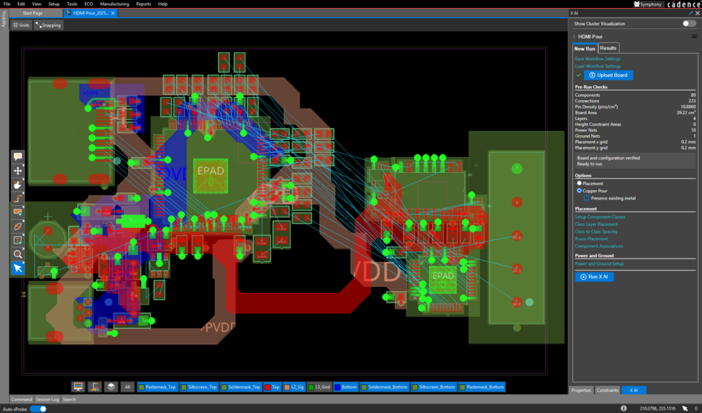
- Built-in workflows and in-design simulation from within your PCB environment to make simulation accessible for all engineers, not just specialists.
- 10x Faster Performance achieved by the new Sigrity X architecture enables rapid turnaround, even for large boards.
- AI-driven optimization with Cadence Optimality™ technology to explore design tradeoffs faster and more intelligently.
- Highly Accurate Solvers maintain hardware-level correlation for reliable signoff.
- Scalable Token Licensing provides a flexible access model that lets teams simulate as needed—without overpaying. Token-based licensing offers scalable and flexible access to all Sigrity capabilities without committing to individual tools.
These features and the integration of simulation into the PCB design flow, generate a new design methodology, creating a simulation-driven design flow.
The Simulation-Driven Design Flow
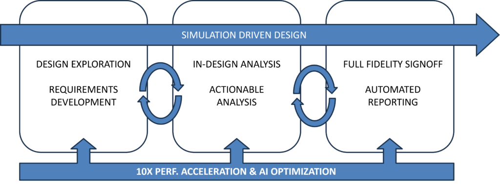
This methodology, enabled by Sigrity X, presents simulation as a continuous flow throughout the PCB development process. With tools like Sigrity X and Optimality, engineers can now build a simulation driven design flow that spans:
- Exploration: To evaluate trade-offs and constraints early using AI-assisted modeling.
- In-Design Simulation: Analyze signal, power, EMI, and thermal behavior while doing place and route enabling you to confirm design decisions as you work.
- Verification and Signoff: Run compliance and correlation-based validation with trusted solvers.
Sigrity X makes it easy to iterate across these simulation stages, allowing you to go back and re-optimize as designs evolve, without redoing everything.
To truly enable this continuous flow, the simulation tools must strike a balance between ease of use and powerful capabilities, making simulation accessible to all designers and producing tangible real-world benefits.
Results from the Field: Real-World Customer Benefits
By implementing a simulation-driven design flow with Sigrity X, several global companies are already seeing measurable gains:
- Microsoft used Sigrity X with Optimality to explore alternative rigid-flex configurations they wouldn’t have considered under time constraints enabling new design possibilities.
- Baidu reduced time spent optimizing transmission line performance by orders of magnitude using AI-guided simulation.
- MediaTek saw a 75% improvement in design performance after integrating Optimality for early-stage optimization.
These results validate the value of combining automation and AI with scalable, accessible simulation workflows.
Final Thoughts
Simulation used to be the domain of experts and corner cases. Sigrity X changes that. Integrating Multiphysics simulation and analysis with Sigrity X into your PCB design process has many proven benefits:
- Ease of Use: Simulation workflows are embedded directly within your PCB CAD tools, enabling interactive simulation like impedance and IR drop analysis without leaving the PCB editor.
- Speed & Scalability: Sigrity X is 10x faster than previous generations and supports parallel processing for faster turnaround.
- AI-Enhanced Optimization: Cadence Optimality uses machine learning to drastically reduce simulation samples while identifying optimal design configurations.
- Token Licensing: Flexible access means users only use what they need making it ideal for teams with variable simulation demands.
With intuitive tools, AI-powered exploration, and flexible licensing, simulation can now become a routine part of the design process, delivering both quality and performance.
The future of PCB design isn’t just about “will it work?” It’s about “what’s the best way to make it work?” With Sigrity X, you don’t have to choose between schedule and certainty, you can have both.
Watch the full webinar, Sigrity X: Reimagining Simulation Driven PCB Design, to learn more about how Sigrity X and Optimality can enhance your PCB design process with integrated simulation and analysis.