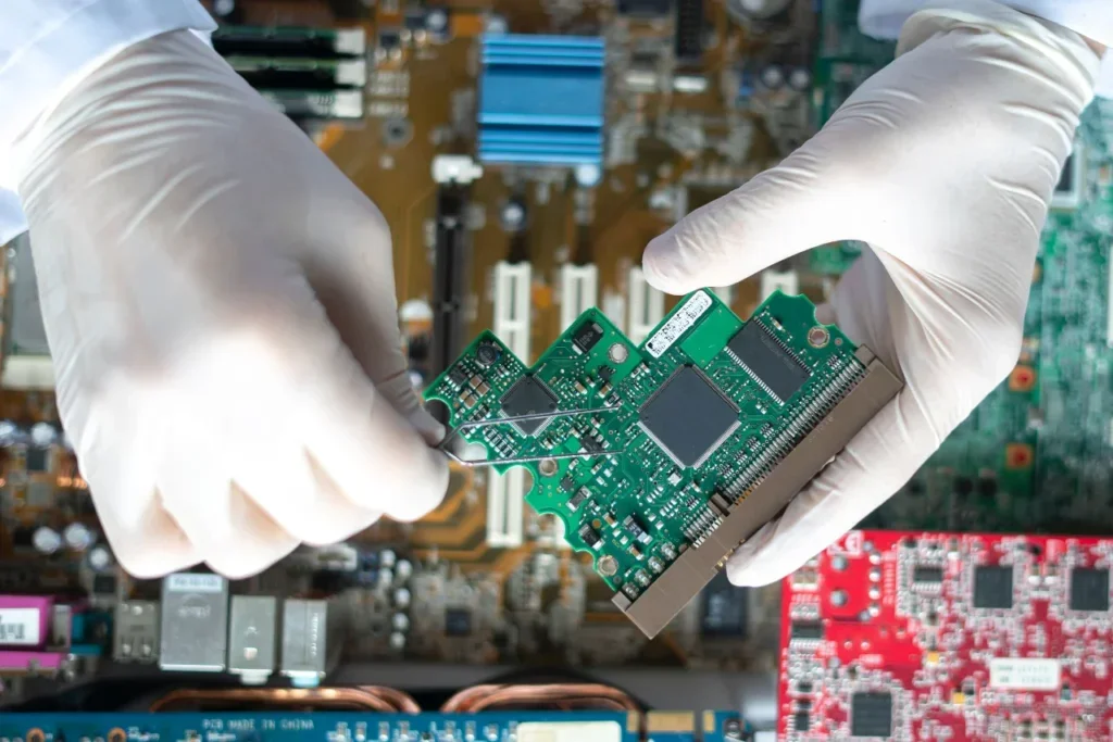
What is the greatest threat to your circuit board meeting its performance objectives? Without a doubt, the answer is electromagnetism. Or more specifically, the effects of electromagnetism, known more affectionately to PCB designers and engineers as electromagnetic interference (EMI), which are inherent attributes of virtually all electronic circuit boards.
EMI is not only a hazard on and within your circuit board, but the area around it, as well. In fact, all electrical and electronic products must exhibit electromagnetic compatibility (EMC), the ability to operate without harming and/or interfering with the operation of other devices, within their operating environment. Therefore, it is critical to understand PCB design for EMI EMC compliance and follow rules and guidelines to achieve it.
Defining EMI and EMC Compliance
EMI and EMC are often referred to as a single issue. These phenomena are indeed interrelated. However, there are distinctions between PCB design for EMI and EMC compliance, as described below, that are helpful to know.
Comparing PCB Design EMI & EMC Compliance | ||
Compliance Issues | EMI Compliance | EMC Compliance |
Area of concern | The surface and layers of the circuit board. | Immediate environment surrounding the PCB or radiation source, especially that includes other electronic devices. |
Non-compliance hazards | Signal degradation, erratic or erroneous operation, system failure | Product malfunction, recalls, legal jeopardy |
Important Standards | None. | 47 CFR Part 15 A, 47 CFR Part 15 B, IEC 61000 Series* |
Objective | To minimize the negative effects of excessive electromagnetism on circuit operation and performance. | To ensure that all electronic devices in the area operate without undue electromagnetic interference from a nearby source |
*IEC 61000 series includes standards based on installation location. These include commercial, industrial, business and industrial environments. There are other industry specific EMC standards; such as IEC 60601-1-2 for medical equipment.
As the table above indicates, there are no specific regulations and/or standards that are limited to the effects of electromagnetism on the board which contains the EMI source. However, onboard EMI is the cause of EMC problems. Therefore, designing PCBs that adhere to EMC compliance standards requires understanding and addressing the sources of EMI on your board.
Understanding EMI and EMC Challenges
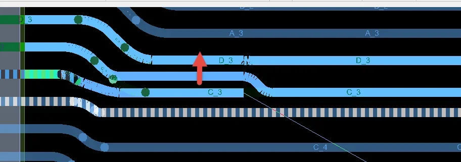
Fundamentally, any movement of charged particles; such as electrons, can create an electromagnetic (EM) field. Therefore, all current carrying elements, whether off-board; such as wire harnesses and common connector cables and wires, or on-board devices; such as components, vias, traces and planes are potential sources of or contributors to EMI. Common sources of EMI on PCBs include the following:
Common Sources of EMI on PCBs
∿ Antennas
∿ Coils and transformers
∿ High power components
∿ Constant and/or simultaneous switching
∿ Common-mode currents
∿ Differential-mode currents
∿ Ground planes
∿ Poor decoupling
∿ Electrostatic discharge
Minimizing disruptive effects, like crosstalk and unintended coupling, from these and other sources on the propagation of RF, digital and power signals on your board and maximizing signal and power integrity is good PCB design. There are several design guidelines, listed below, that if implemented will help you mitigate the effects of EMI.
Guidelines for Mitigating EMI on Your PCB
|
Following the guidelines will not eliminate EMI; however, they will significantly reduce the EM issues on your board and help you satisfy EMC requirements. Many of the suggestions above relate to PCB stackup design, which is a primary consideration for multilayer board design. For more information on PCB stackup design for EMI EMC compliance, check out this webinar on How to Design Your PCB for Low EMI.
Meeting the design objective of low EMI, while simultaneously making sure the radiation from your board adheres to regulations and standards, can be daunting. Successfully achieving these goals, while ensuring your board’s operation does not interfere with the operation of nearby electronic systems or products is the challenge of PCB design for EMI EMC compliance.
Achieving PCB Design EMI EMC Compliance
EMI EMC compliance is not simply a goal for good PCB design. Failing to achieve this objective can delay product launch, prevent entry into some markets or have significant cost consequences for returns, replacements and/or legal judgments. Therefore, it is imperative to employ a strategy, as listed below, to reach or exceed the requirements for compliance.
PCB Design for EMI EMC Compliance
✅ Understand the causes and sources of EMI and EMC
✅ Identify the specific EMI and EMC challenges for your design
✅ Follow good EMI mitigation design guidelines
✅ Employ PCB EMC simulation software to verify your design meets
standards requirements before manufacturing
Adopting the strategy as listed will help you achieve PCB design EMI EMC compliance and avoid costly contingencies.
EMA Design Automation is a leading provider of the resources that engineers rely on to accelerate innovation. We provide solutions that include PCB design and analysis packages, custom integration software, and engineering expertise, which enable you to create more efficiently. For more information on achieving PCB design EMI EMC compliance and how we can help you or your team innovate faster, contact us.