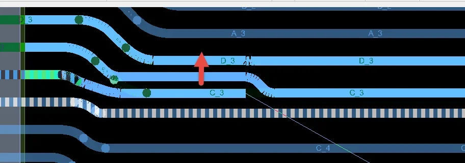
Arguably, routing traces is the most challenging task of laying out your circuit board. In addition to meeting the basic mandate of ensuring all connections are made, there are constraints that must be adhered to and guidelines that should be followed. For example, satisfying creepage and clearance standards is required and methods to reduce crosstalk and maximize signal integrity need to be implemented.
Fortunately, there is design rule checking (DRC) that provides alerts when rules and constraints are violated. Troubleshooting these errors is often a trial-and-error process that can be time-consuming and costly–in terms of increased design time and expense. The best way to minimize rules violations and satisfy routing requirements more efficiently is to employ PCB design software with auto routing.
Methods for Routing PCB Traces
Basically, there are three routing options for PCB layout design, as listed below.
| PCB TRACE ROUTING TECHNIQUES | ||
| Routing Technique | Description |
Advantage/ Disadvantage |
| Manual routing | For manual routing, the designer runs all traces and creates all pin connections on the circuit board layout without program assistance. | Designer has complete control over process. / Slowest. |
| Automatic routing | Automatic routing is when the EDA program’s autorouter performs all trace routing according to a previously created hierarchy of rules and constraints. | Fastest and most accurate./ Designer has no process control. |
| Auto-interactive routing | Auto-interactive routing is when the designer manually routes the board with assistance from an autorouter. For example, to create meanders to ensure impedance matching for differential traces. | Fast, accurate and allows for special considerations./ Depends on designer for correct pin connections. |
| AI auto routing | AI routing incorporates the advanced search and decision making capabilities of generative AI to compare and contrast placement and routing (P & R) options and create the PCB layout many times faster than other techniques. | Exceptionally fast, combines placement and routing into one layout step./ Depends on rules definitions to ensure SI/PI are maximized. |
Although complete control may sound nice, manual routing is probably the worst option for today’s complex circuit board designs. Not only is manual routing slow, but it is the most difficult and likely to generate the most errors requiring the most time to troubleshoot. For these reasons, virtually all EDA development companies offer PCB design software with auto routing to some degree.
How PCB Autorouters Work
All PCB autorouters have the same objective. Specifically, to route traces according to the hierarchy of rules that you have defined, which should adhere to industry standards and incorporate design for manufacturing and assembly (DFMA) guidelines, with the least or no errors/conflicts. However, there are several types of auto routing, listed below, for achieving this goal.
PCB Design Software with Auto Routing Types
- Gridless
- Topological
- Pattern
- Channel
- Line-probe
- Maze
The list above is not exhaustive, yet it illustrates there are multiple approaches that can be taken to auto routing a circuit board. Irrespective of the specific type of scheme, PCB autorouters typically follow a common algorithmic pattern.
|
PCB Autorouting Paradigm
|
Variations to this algorithm are utilized by different PCB design software with auto routing programs. This include, different clean-up methods and even rule modification schemes to avoid divergence where no error-free layout can be attained.
PCB Design Software with Auto Routing Optimization
Successfully routing your board–such that no rule violations remain–is not required to complete your design and send off for fabrication and assembly. However, failing to achieve this level of PCB design verification can lead to substandard builds and/or low-quality boards. In some cases, your board may not be manufacturable at all without redesign. These contingencies can be avoided by following PCB layout optimization guidelines; such as listed below.
Optimizing Your PCB Design Software with Auto Routing Utilization
- Acquire and incorporate your CM’s DFMA rules into your Constraint Editor.
- Follow good PCB layout design best practices
- Opt for auto-interactive routing for fast, accurate and editable trace routing
- Employ real-time DRC
Virtually all circuit board design programs today include some level of automatic routing. However, choosing an advanced PCB Design EDA tool that includes real-time auto-interactive routing will ensure that you avoid contingencies that will delay board development and increase costs.
EMA Design Automation is a leading provider of the resources that engineers rely on to accelerate innovation. We provide solutions that include PCB design and analysis packages, custom integration software, engineering expertise, and a comprehensive academy of learning and training materials, which enable you to create more efficiently. For more information on PCB design software with auto routing and how we can help you or your team innovate faster, contact us.