
As circuit board size decreases and functionality and capability demands increase, circuit board real estate becomes extremely valuable. Footprint pads, part pins, traces, vias, and other circuit board elements all need adequate space. Not to mention, circuit board fabrication and PCB assembly processes that require spacing for solder masking, solder flow, depanelization, etc. For high-voltage circuit boards, adequately addressing spacing is even more critical due to the significant damage that large voltages, currents and powers can create.
Consequently, there are regulations and guidance that emphasize the need for adequate spacing between conductive elements is in place. This is especially true for multilayer PCB designs, where increased layers are used to support smaller board area sizes. Fortunately, there are industry organizations that regularly publish rules and guidelines to address spacing on PCBAs, including creepage and clearance standards that are focused on trace routes. Knowing and following these standards is a key to designing safe boards that satisfy your performance objectives and will reliably perform over their lifecycle.
The Creepage and Clearance Standards to Know
The most common considerations with any board design for engineers throughout the PCBA design process are how to minimize electromagnetic interference (EMI) and maximize electromagnetic compatibility (EMC). For high-voltage applications, EMI or unwanted noise and excessive emissions–a major EMC issue–are also important. However, at elevated voltage/current/power levels, safety is the greatest concern.
High voltages can be the catalyst for damaging surface tracking, where an alternate current path between conductors is created through the board’s insulation. These “effective short circuits” can damage components, the PCB and lead to fires that threaten other boards, systems and even nearby users.
The most effective means of mitigating these contingencies is to have sufficient distance between sources and potential areas that can be affected. Consequently, there are several industry publications that include recommendations, guidelines, and/or requirements for PCB creepage and clearance distances. The most important of these are listed below.
*Replaces the well-known IEC-60950-1 Information Technology Equipment standard.
The publications listed above are not exhaustive creepage and clearance standards for all circuit board designs. However, they do contain industry requirements that are applicable to the most common PCBA design types, where EMI, EMC, and safety are primary considerations. In addition to knowing what creepage and clearance standards to use, it is also essential to understand the difference between creepage and clearance for circuit boards.
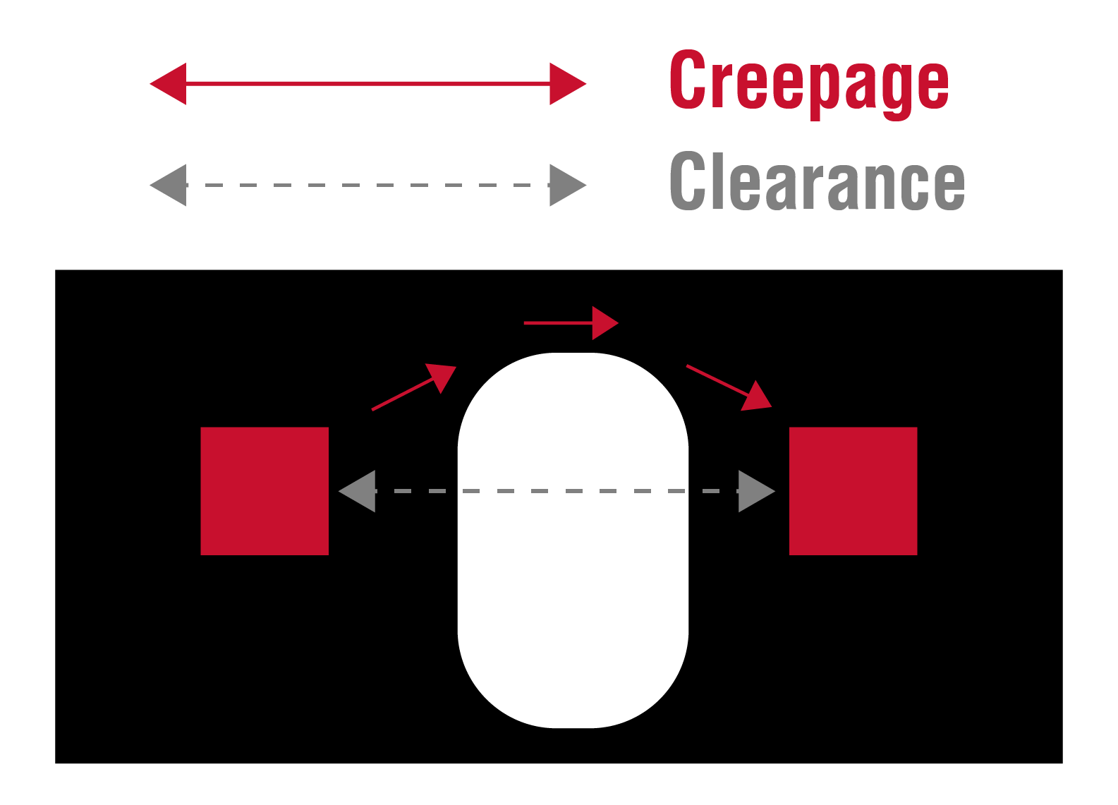
Above, creepage and clearance refer to the distance between any conductive board elements. For example, this includes trace to trace, conductor pad to trace, via annular ring to pad, etc. Often, the clearance distance is shorter than the creepage distance due to trace routing around board obstacles, such as components or drill holes.
PCBA Creepage and Clearance Design Best Practices
Spacing requirements are an essential part of your CM’s DFMA rules and guidelines that should be integrated into the PCBA design process. Doing so is essential for the manufacturability of your board. These rules should include and/or be consistent with industry creepage and clearance standards, which can be ensured by following the best practices listed below.
Creepage and Clearance Design Guidelines
- Determine which creepage and clearance standards and distances apply to your board type
- Setup your PCB design software DRC creepage and clearance constraints according to the appropriate standard specification(s)
- Perform DRC checks often and correct any spacing violations identified during your PCB layout design process by
- Adding a slot between conductors to increase creepage distance without modifying the locations of any conductors
- Adding vertical insulation barrier between conductors to increase creepage distance
- Changing the orientation of a conductive element–this may require rerouting traces
- Replacing the conductor with an alternative part with similar performance criteria
- Use PCB simulation to check/verify that your creepage and clearance specifications meet industry safety standards for all voltage levels
By following the guidelines above, including adhering to the distance constraints from the proper industry creepage and clearance standards, you can make sure your board is designed to maximize component, board and user safety, as well as minimize issues like EMI and meet your performance objectives. This is best accomplished by utilizing an advanced PCB design package or incorporating a product design software solution that includes dedicated functionalities–for example, creepage and clearance vision with color-coded overlays–to help you optimize your development process.
EMA Design Automation is a leading provider of the resources that engineers rely on to accelerate innovation. We provide solutions that include PCB design and analysis packages, custom integration software, and engineering expertise, which enable you to create more efficiently. For more information on how best to incorporate PCB creepage and clearance standards into your design process and how we can help you or your team innovate faster, contact us.