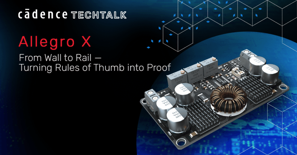
As an EMC consultant, Kenneth Wyatt has seen a lot of PC board designs and associated product EMC compliance failures. This includes not only the very common radiated emissions failures, but radiated immunity and ESD failures, as well. Most compliance issues tend to share a common root cause – the PC board stack-up design. Most stack-up designs are created by “rules of thumb” which are often outdated. We will learn why these rules no longer apply and how to correctly design your next PC board stack-up. He will explain the physics of digital signal propagation as electromagnetic waves and how this will help dictate proper stack-up and circuit routing design for lowest EMI issues.