Simple circuit board layouts can be readily created manually. However, the complexity of most layouts dictate that your EDA program includes features like auto routing for efficient design. However, there are other important attributes that should guide you when selecting a PCB design program. To aid you, we have compiled free and paid lists of the best PCB layout design software tools that exhibit the important attributes to consider for effective design and development
Best PCB Layout Design Software
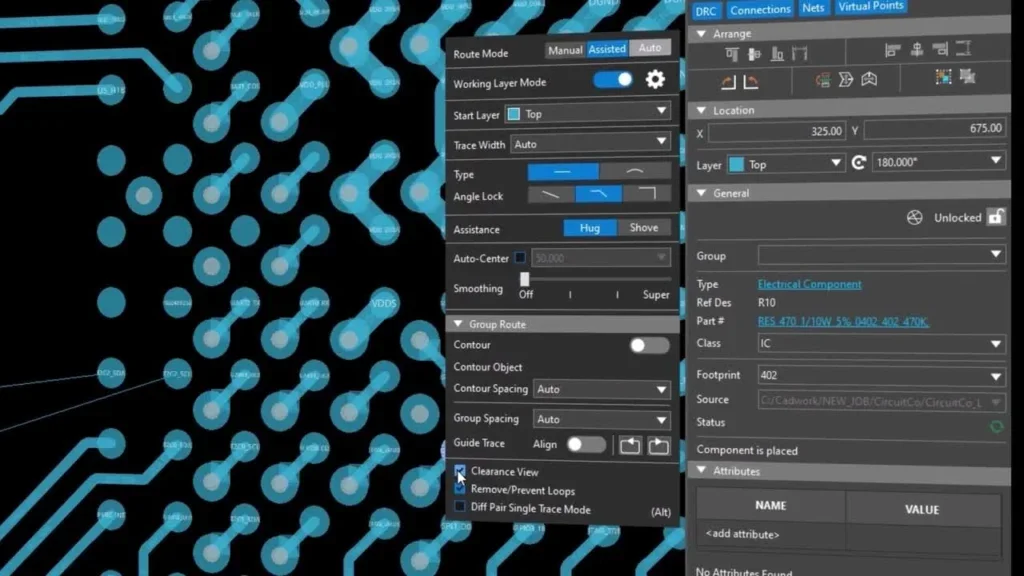
There is no shortage of PCB design software programs from which to choose. This includes both free and paid CAD tools that meet the basic requirements for board design, but run the gamut in terms of capabilities. As PCB layout is one of the two primary stages of electronic circuit board design, it is important that functionalities and attributes that support board layout guide your selection of which EDA tool to use.
Below, the best PCB layout design software based on properties that impact layout creation are listed.
BEST PCB LAYOUT DESIGN SOFTWARE | ||
Rank | Free PCB Layout Software | Paid PCB Layout Software |
| 1 | ||
| 2 | EasyEDA | |
| 3 | PADS | |
| 4 | ||
| 5 | ExpressPCB | |
The lists above are not exhaustive. However, they are representative of the best PCB layout tools available for circuit board designers and engineers whose experience may range from novice to expert.
Best Free Software for PCB Layout
KiCAD
KiCAD is a preferred PCB design program for students and inexperienced board designers. Although the EDA tool is free, it comes with all the necessary capabilities to design low to moderately complex circuit boards. PCB layout design strengths include:
- Intuitive PCB editor UI
- Interactive trace routing capability
- Dedicated high-speed trace pruning tool
- PCB-schematic cross-probe functionality
EasyEDA
EasyEDA is a popular free PCB design program among new designers and early career engineers due to its ease of use, component placement and PCB editing features. The ability to access the tool from anywhere online has long been a popular attribute–with many PCB programs migrating to the cloud, this feature is less distinctive than it once was. Program strengths include:
- Large component library
- Simple component placement
- Easy to use PCB editing interface
- User command creation and/or customization
PCB123
One of the best PCB layout design software programs for free is PCB123. PCB123 is on par with many paid EDA tools in terms of capabilities and features. However, this tool is intended for use by Sunstone customers. Therefore, import/export options are limited. Strengths include:
- Board design without schematic capture
- Full-function PCB layout editor
- Detailed 3D rendering
- Free DFM verification
CircuitMaker
CircuitMaker, which is built on the same engine as Altium Designer, is a good free PCB design program for hobbyists, students and early career engineers. All the necessary features for designing simple-to-moderately complex circuit boards are included. CircuitMaker is also a good program to learn in preparation for upgrading to a more advanced paid PCB layout design software tool. Notable features are:
- Topological autorouter
- Interactive auto routing capabilities
- Interactive 3D rendering
- DFC/DFM validation
ExpressPCB
ExpressPCB Plus is a dedicated PCB layout program. The program is free and simple to use. The tool is lauded for the simplicity of creating components; including footprints for the board layout. Features include:
- Easy to use UI
- Intuitive and simple platform
- Good for novices and students to learn PCB layout
Best Paid Software for PCB Layout
OrCAD X
OrCAD X is the industry standard for PCB design software. The program includes advanced capabilities for PCB layout, as well as unparalleled simulation and analysis integrations; such as ECAD-MCAD co-design, to help you optimize your individual or team electronic product development process. Features include:
- Next Generation High performance PCB UX
- Real-time design analysis
- Integrated supply chain insights
- Automated manufacturing documentation & RTM packaging
Altium Designer
Altium Designer is one of the industry’s most popular and capable PCB design programs. Although equipped with advanced PCB layout capabilities, the software panel layout makes using the tool fairly straightforward. Features include:
- Interactive routing functionality
- Ready to use stackup templates
- Real-time supply chain data
- Intuitive multi-board connectivity tool
PADS
PADS, by Mentor Graphics, is also a highly functional PCB design software program. The program integrates with other tools for efficient development. For PCB layout design, PADs has the following capabilities:
- Automatic routing capabilities
- Multi-trace high-speed routing functionality
- Rigid-flex board layout design
- ECAD-MCAD co-design
Autodesk Eagle
Autodesk Eagle, once a free EDA tool, is still a low-cost popular program. The software is integrated into the Autodesk Fusion 360 platform, which allows for seamless ECAD-MCAD design and development. For PCB layout, the following features are notable.
- Adaptive interactive routing
- Obstacle avoidance routing
- Layout object alignment functionality
- Real-time schematic and layout synchronization
DipTrace
DipTrace is known for its easy component library–schematic symbol and footprint–creation capabilities. This ease of use is pervasive throughout the program, especially for PCB layout design. The following features are included.
- Multiple component placement options
- High-speed shape based autorouter
- Smart copper pour and auto fanout functionalities
- Real-time DRC
Optimizing Your PCB Design and Development
As shown above, options for PCB layout capabilities range from the industry’s most advanced EDA design tools to free programs for less complex designs, and/or honing your PCB design process skills. PCB layout is arguably the most important stage of PCB design; however, there are other tools that can help you optimize your board development process. These product design and development software tools provide simulation and analysis to verify signal integrity and power integrity (SI/PI), ensure EMI and EMC compliance and other performance and operational verification that minimize manufacturing turnaround time and costs. Partnering with an industry leader in providing these integrated solutions, coupled with choosing the best PCB layout design software for you is the path to PCB design and development optimization.
EMA Design Automation is a leading provider of the resources that engineers rely on to accelerate innovation. We provide solutions that include PCB design and analysis packages, custom integration software, and engineering expertise, which enable you to create more efficiently. For more information on choosing and effectively using the best PCB layout design software and how we can help you or your team innovate faster, contact us.