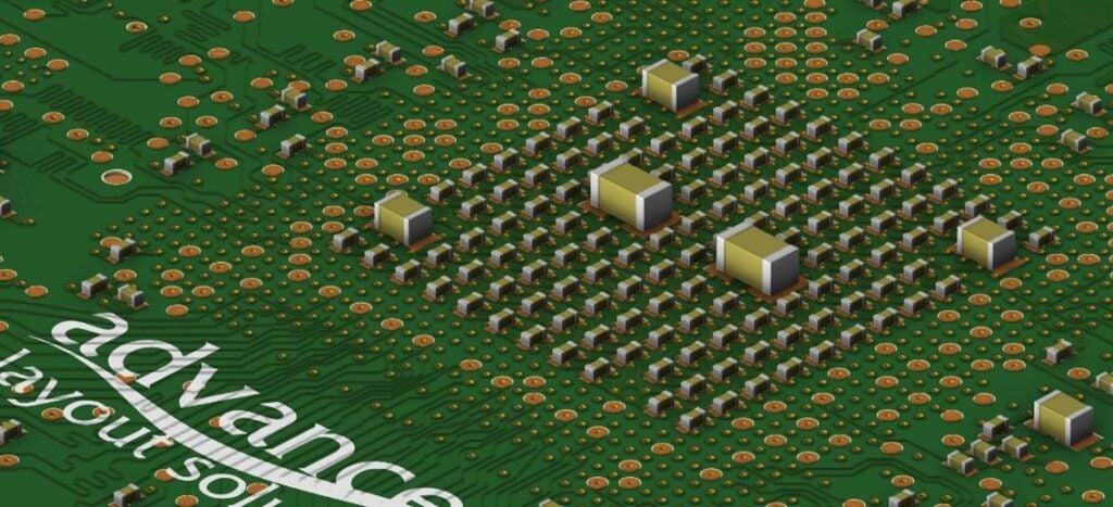
ALS Solves High-Speed PCB Design Challenges with Cadence Sigrity X
ADVANCED LAYOUT SOLUTIONS, the UK’s largest design bureau that specializes in high-speed printed circuit board development, has revolutionized their design process and achieved unprecedented success using Cadence Sigrity Signal Integrity and Power Integrity tools. While bound by non-disclosure agreements that prevent discussing specific client projects, ADVANCED LAYOUT SOLUTIONS’s lead engineer, Chris Halford, shared insights into how Sigrity has transformed their capabilities and results.
“Cadence Sigrity has become an indispensable part of our high-speed PCB design workflow. The comprehensive suite of analysis tools has allowed us to tackle increasingly complex designs with confidence, reducing iterations and time-to-market for our clients.”
Chris Halford – Advanced Layout Solutions, ALSPCB | Advanced Layout Solutions Website
“The ability to simulate and analyze signal and power integrity issues early in the design process has been particularly valuable, helping us to identify and resolve potential problems before they become costly setbacks.
We have access to all the major Sigrity SI and PI tools via the Cadence Sigrity token system – a genius way to access all the Sigrity tools as we wish – each Sigrity tool requires a certain number of tokens to access and once you close the software it releases the tokens to be used on other Sigrity tools.
Knowing that we have access to the latest tools and expert support from Parallel Systems and Cadence, gives us confidence to take on challenging projects and deliver exceptional results for our clients.
The Sigrity suite’s intuitive interface and comprehensive features have empowered our team to push the boundaries of PCB design. We’ve been able to optimize power delivery networks and ensure reliable performance in increasingly dense and high-frequency boards.
Cadence Sigrity tools have not only enhanced our capabilities but also strengthened our reputation as a go-to partner for challenging high-speed PCB projects. We look forward to continuing our success with Cadence as we tackle the next generation of electronic designs.”
Key Features of Using the Cadence Sigrity Suite:
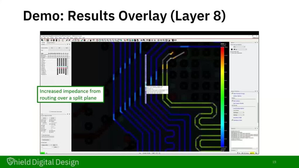
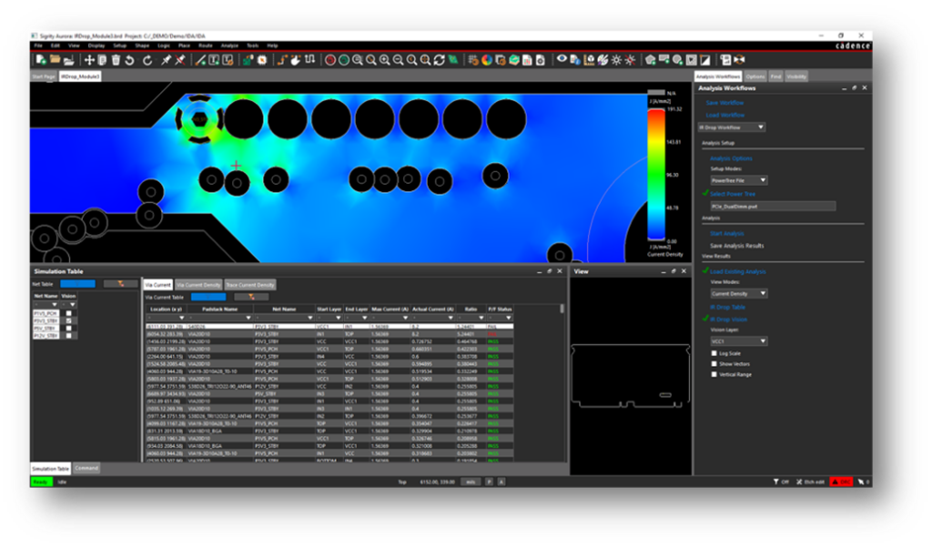
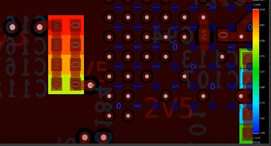
Early SI/PI Problems Detected During Layout
Signal Integrity (SI) and Power Integrity (PI) analysis can be performed during the PCB layout to pinpoint potential problems, make informed decisions, and optimize the design when change is easiest. SI and PI simulations can be accessed directly in the PCB canvas, with results overlayed on the board to easily visualize results and identify common SI/PI problems.
Key Aspects of Early SI/PI Analysis with Sigrity
During the early stages of PCB layout, we frequently utilize PowerDC for power integrity (PI) simulation purposes. This process helps to:
- Assess the need for additional layers
- Evaluate the adequacy of the current layer structure
- Optimize copper weights
- Determine if power layer reduction is feasible
Benefits of Early SI/PI Analysis with Sigrity
Performing early signal integrity and power integrity simulations during the PCB layout often leads to more efficient designs, sometimes revealing opportunities to use lower copper weights or reduce the number of power layers.
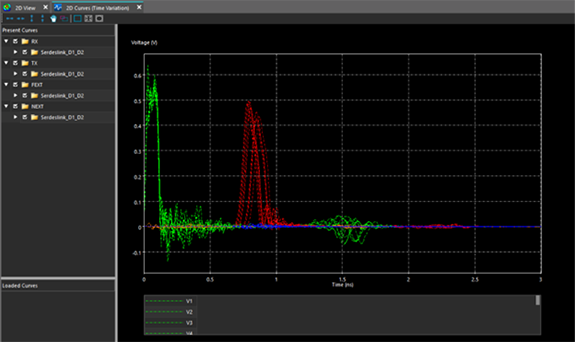
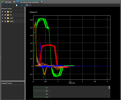
SI Signoff of DDR Interfaces
For SI signoff of DDR interfaces, a hybrid solver approach is preferred over full 3D extraction. While 3D extraction using tools like Clarity can provide highly accurate S-parameter models, it is far more practical to rely on the workhorse capabilities of the hybrid solver for day-to-day simulations. However, it is good to know that on very high-speed memory buses or in cases where margins are quite tight, the speed and capacity of a 3D extraction tool like Clarity can be called upon for final signoff.
Key Aspects of SI Signoff of DDR Interfaces
The hybrid solver method offers a balance of accuracy and efficiency:
- It considers both non-ideal data signals and the non-ideal power delivery network
- It allows for rapid analysis and assessment of power-aware SI issues without repeated model extraction
- It can handle the complexity of DDR interfaces, including high routing density, length matching, spacing, and data signal grouping
Benefits of SI Signoff for DDR Interfaces
While full 3D solvers can be used for final signoff, day-to-day analysis requires quick but accurate results which can be used to verify performance and improve functionality. Using Sigrity for SI signoff of DDR interfaces, you can:
- Address the challenges of large DDR buses with numerous signals, power/ground nets, and decoupling capacitors
- Achieve more accurate simulation results that match lab results
- Obtain a quicker time to market
- Perform simulation and analysis of hundreds of ports often required in advanced multi-chip DDR interfaces
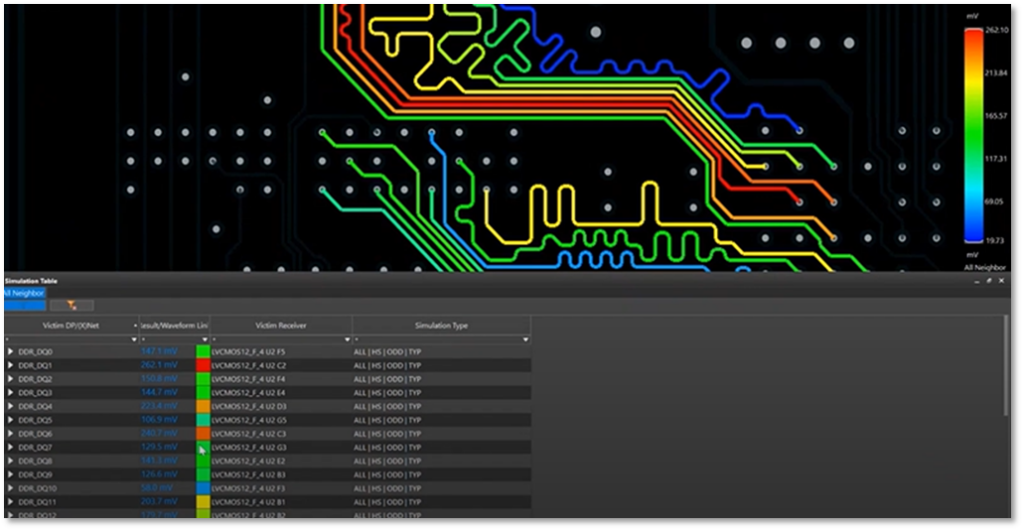
For final signoff, accuracy remains crucial. However, for most cases, extracting entire memory buses with power and ground in 3D can be relegated to a back plan to the hybrid solver. The hybrid solver strikes a balance, providing sufficient accuracy for signoff without the computational overhead of full 3D extraction. However, in extreme cases, a memory efficient and fast 3D solver like Clarity, can step in and provide the extra assurance required to signoff on DDR interfaces.
Via Structure Optimization
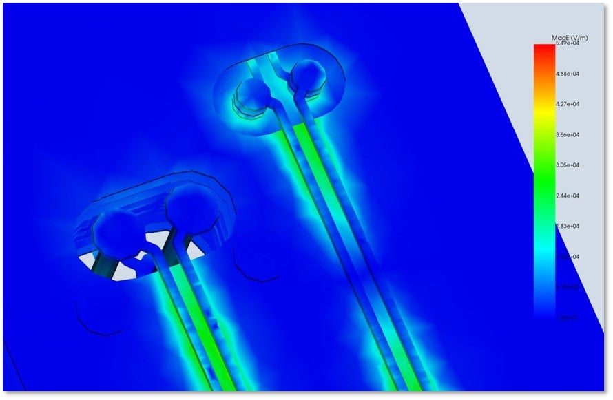
Key Aspects of Via Structure Optimization with Clarity
We regularly use Clarity to simulate and optimize via structures for high-speed channels early in the design process. This practice ensures that:
- The PCB designer incorporates properly designed, low-loss vias from the outset
- Signal integrity is considered proactively rather than reactively
- Potential issues are identified and addressed early, reducing the need for late-stage interventions
Benefits of Via Structure Optimization with Clarity
Performing via structure optimization with Clarity has proven beneficial in enhancing overall design quality and reducing the likelihood of SI-related problems later in the development cycle.
Power Integrity Signoff Including Transient E/T Co-Simulation
Power integrity signoff is a critical step in the design, particularly for System-on-Chip (SoC) designs. It involves both static and dynamic analysis of the power grid. Static analysis helps identify weak spots in the power network, while dynamic analysis simulates the behavior of the grid under various operating conditions. IR drop analysis ensures that voltage levels across the chip remain within acceptable ranges, preventing performance degradation or functional failures.
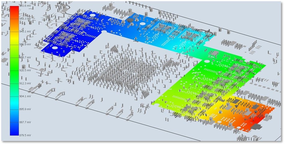
Key Aspects of Power Integrity Signoff with Celsius Thermal Solver
Performing IR drop analysis and incorporating transient E/T co-simulation, enabled by tools like the Celsius Thermal Solver, is critical to power integrity signoff. Taking both electrical and thermal considerations into the evaluation allows us to:
- Analyze the dynamic thermal behavior of the chip
- Identify hotspots and thermal gradients
- Assess the impact of temperature on electrical performance
- Optimize the power delivery network for both electrical and thermal considerations
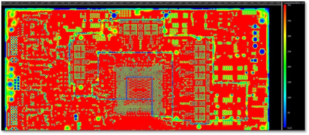
Benefits of Advanced Power Integrity Signoff with Celsius Thermal Solver
Performing advanced power integrity signoff with Celsius Thermal Solver improves the PCB design process and helps to create a robust and reliable power delivery network. Benefits include:
- Improved reliability and performance of SoCs
- Reduced risk of chip failures due to power-related issues
- Optimized power delivery network design
- Enhanced understanding of chip behavior under various operating conditions
By incorporating transient E/T co-simulation into the power integrity signoff process, designers can achieve a more comprehensive and accurate analysis of their SoC designs, leading to more robust and efficient chips.
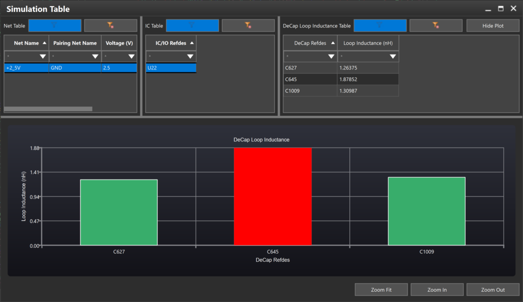
Decoupling Capacitor Optimization
Sigrity OptimizePI offers several advantages for decoupling capacitor optimization, balancing cost and performance.
Key Aspects of Decoupling Capacitor Optimization
- Performance optimization: The tool ensures high performance for the power delivery system at both system and component levels
- Elimination of over-design: The tool helps eliminate unnecessary decaps, reducing over-design for PCBs and IC package
- Design area recapture: By removing unnecessary decaps, OptimizePI helps reclaim valuable design space
- Interactive cost vs. performance assessment: Users can interactively evaluate trade-offs between PDS cost and performance
- Optimization across board/package interface: The tool optimizes PDS across both board and package interfaces.
- Flexibility: The tool can be configured to maximize performance or reduce decap area without regard for cost, depending on specific needs
- Timesaving: By automating the optimization process, OptimizePI can significantly reduce PCB development time.
Benefits of Decoupling Capacitor Optimization with Sigrity
The advantages obtained by performing decoupler capacitor optimization allow the design team to achieve an optimal balance between decoupling capacitor cost and performance, resulting in more efficient and cost-effective designs.
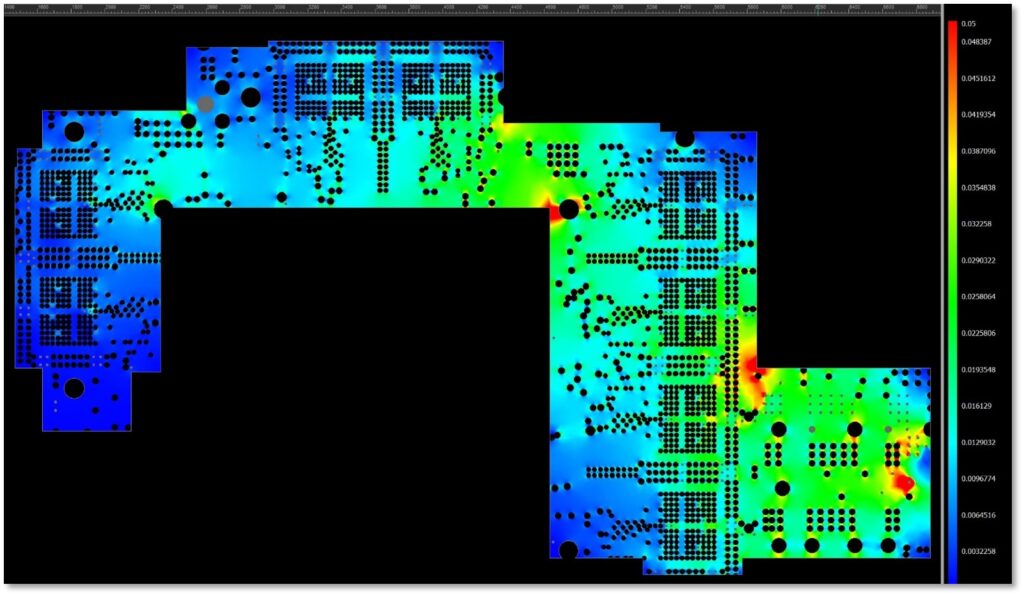
Multi-Board Power Integrity Signoff
Multi-board power integrity signoff using SystemPI is an advanced analysis technique for ensuring proper power delivery across interconnected PCBs.
Key Aspects of Multi-Board PI Signoff
Multi-board PI signoff can be used for power integrity analysis of the full system with:
- Power Delivery Network Analysis: Evaluates the entire power distribution system across multiple boards, including VRMs, power planes, and decoupling capacitors
- DC Analysis: Ensures adequate voltage and current delivery to components on all boards
- AC Analysis: Addresses transient current demands and high-frequency power delivery requirements
- Inter-board Connections: Analyzes connectors and interfaces between boards for potential PI issues
Benefits of PI Signoff with Sigrity
Power integrity is often overlooked, but it’s critical for high-speed designs. Sigrity’s PI tools have helped us avoid many potential issues that could have led to mysterious signal integrity problems or EMI failures down the line.
Addressing High-Speed Design Challenges with Sigrity
“Cadence Sigrity has been a key factor in our growth and success. It has allowed us to differentiate ourselves in the market and deliver superior results for our clients. We consider it an essential tool for any serious high-speed PCB design team.”
Chris Halford – Advanced Layout Solutions, ALSPCB | Advanced Layout Solutions Website
With Sigrity, ALS performed simulation and analysis throughout multiple stages of the PCB design process to:
- Identify common signal integrity and power integrity problems
- Make informed design decisions
- Optimize elements of the PCB layout
- Verify performance of high-speed signals
- Perform final SI/PI signoff
ALS was able to deploy Sigrity to solve their high-speed and complex design challenges with upfront multi-physics simulation, saving their customer time and ensuring first pass success.