AI can be used to accelerate your PCB design process, quickly providing options for component placement, copper pours, or routing to jump start your PCB layouts; however, when incorporating AI, it is important to provide clear and concise guidelines to generate a board that is functional and manufacturable. For best results, designers should configure constraints and certain settings within your PCB design software to prevent errors or violations during AI-generated placement or routing.
This quick how-to will provide step-by-step instructions on how to configure constraints and the required design settings to improve AI-generated results using Allegro X AI in OrCAD X.
To follow along, download the provided files above the table of contents.
How-To Video
 Open in New Window
Configure Constraints for X AI: Placement Rooms
Note: Rooms can be used during AI-generated component placement to keep critical circuitry together and connections short. The following steps will discuss how to draw rooms on your PCB design. If rooms are defined in the schematic but not drawn on the PCB, X AI will place components in a “floating” room. Learn how to define rooms in the schematic here.
Step 1: Open the provided design in OrCAD X PCB Designer.
Step 2: Component rooms are utilized with XAI component placement. Rooms have been defined for the components in this design during schematic creation. To define room areas on the board, select Shape > Rectangular from the menu.
Step 3: In the Options panel, set the Active Class to Board Geometry and the Active Subclass to Both_Rooms.
Step 4: Right-click the upper-left corner of the board package keepin and select Snap Pick To > Segment Vertex.
Step 5: One corner of the shape is attached to the corner and the other is attached to your cursor. Move the mouse to the center of the board to create a rectangle in the upper-left corner.
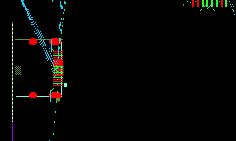
Step 6: Click to place the rectangle.
Step 7: Repeat steps 4-6 for another rectangle in the bottom-left corner and a larger rectangle on the right half of the board. When finished, right-click and select Done.
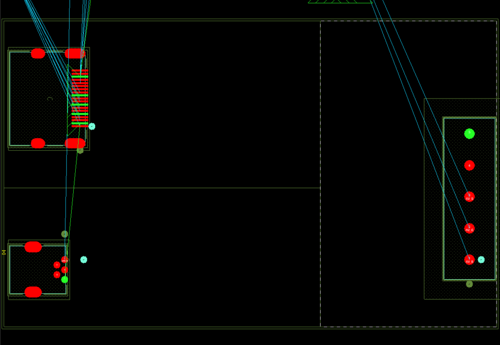
Step 8: To assign names to each room, select Add > Text from the menu.
Step 9: In the Options panel, set the active class to Board Geometry and the active subclass to Both Rooms. Set the Text Block to 6.
Step 10: Select the upper-left room to define it as the active room for the text.
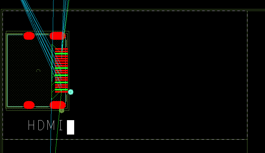
Step 11: Click anywhere inside the room to start writing the text. Enter HDMI for the room name. When finished, click outside the room to deselect the text.
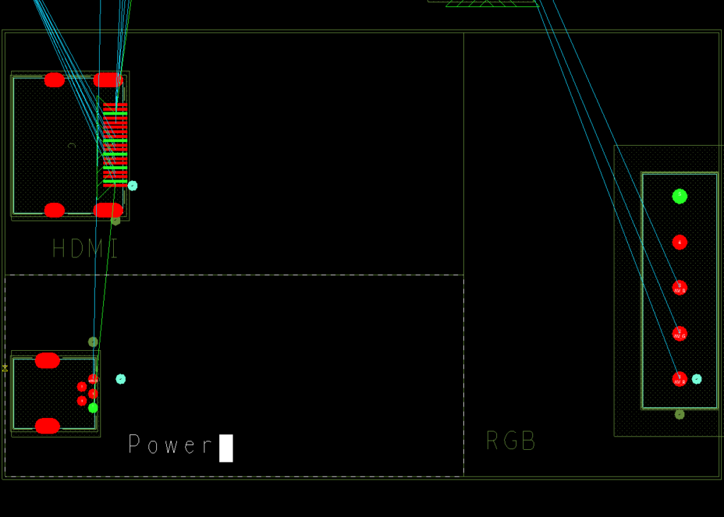
Step 12: Repeat steps 10 and 11 for the other two rooms. Name the rightmost room RGB and the bottom-left room Power. When finished, right-click and select Done.
Configure Constraints for X AI: Assign Differential Pairs
Step 13: For copper plane generation, plane spacing must be defined in the Constraint Manager. Select Setup > Constraints from the menu.
Step 14: The Constraint Manager window opens. Select the Electrical domain from the worksheet selector.
Step 15: Expand and select the Net > Routing > Differential Pair worksheet.
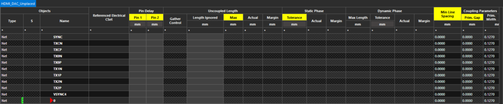
Step 16: Scroll to the bottom of the net list to view the HDMI data nets. These nets can be designated as differential pairs to ensure they are routed together and that all differential pair constraints apply.
Step 17: Right-click one of the nets and select Create > Differential Pair.
Step 18: The Create Differential Pair window opens with the net listed. Select Auto Setup to designate all HDMI differential pairs simultaneously.
Note: To learn how to define a differential pair manually, see our how-to here.
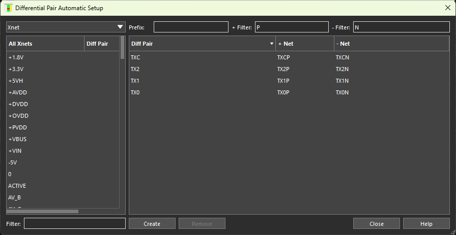
Step 19: The Differential Pair Automatic Setup window opens. Enter P for the positive filter and N for the negative filter. Click outside the text fields. The differential pair table is populated with potential differential pairs TXC, TX2, TX1, and TX0. These are the HDMI data lines to be balanced.
Step 20: Click Create to create the differential pairs. A log file opens, showing the pairs created and their associated nets. Close the log file.
Step 21: Click Close in the Differential Pair Automatic Setup and Create Differential Pair windows.
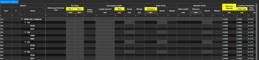
Step 22: Back in the Constraint Manager, scroll to the top of the net table. The HDMI nets are shown as differential pair objects.
Configure Constraints for X AI: Physical Rules
Step 23: To define physical constraints, select the Physical domain from the Worksheet Selector.
Note: X AI will honor the following physical rules during layout generation:
- Layer sets and assignments
- Minimum line width
- Differential pair minimum line spacing
- Differential pair primary gap
- Vias
- All pad-pad connect
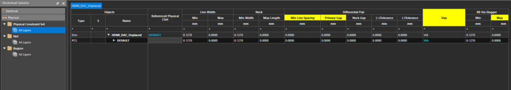
Step 24: Select the Physical Constraints > All Layers worksheet. A table of physical constraint sets is shown.
Note: These constraint sets can be assigned to multiple nets.
Step 25: Right-click the Default constraint set and select Create > Physical CSet from the menu.
Step 26: Enter PWR_GND for the constraint set name and click OK to create the set.
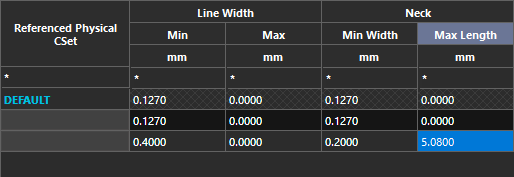
Step 27: The constraint set is added to a new row in the table. Define the following parameters for the new set:
- Minimum Line Width: 0.4
- Minimum Neck Width: 0.2
- Maximum Neck Length: 5.08
Step 28: Right-click the DEFAULT constraint set again and select Create > Physical CSet. Enter DP for the constraint set name and click OK.
Step 29: Define the following parameters for the DP set:
- Minimum Line Spacing: 0.127
- Primary Gap: 0.2
Step 30: To assign physical constraint sets, select the Net > All Layers worksheet from the Physical domain.
Step 31: A new table is shown with a list of nets and their assigned physical constraints. Click and drag the cells under Referenced Physical CSet for the HDMI differential pairs TXC and TX0-TX2.
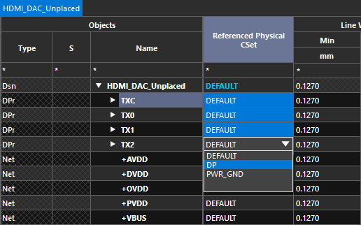
Step 32: Select DP from the resulting dropdown. The DP constraint set is assigned to the differential pairs.
Step 33: Click and drag the cells under Referenced Physical CSet for the power nets and select PWR_GND from the resulting dropdown.
Note: All power net names start with a plus or minus sign to ensure they are lined up sequentially in the Constraint Manager so all can be selected at once.
Step 34: Scroll down and select the Referenced Physical CSet cell for ground net 0. Select PWR_GND from the resulting dropdown. Physical constraint sets have been assigned.
Configure Constraints for X AI: Spacing Rules
Step 35: To define spacing rules, select the Spacing domain from the worksheet selector.
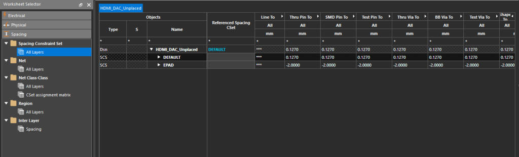
Step 36: Select the Spacing Constraint Set > All Layers worksheet. A table of spacing constraints opens in the Constraint manager window.
Step 37: Scroll to the defined Shape To Shape spacing in the Default constraint set and select the cell to edit it.
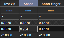
Step 38: Enter 0.254 for the shape-to-shape spacing and click outside the cell.
Note: X AI will honor the following spacing rules during layout generation:
- Line to
- SMD Pin To
- Test Pin To
- Thru Via To
- BB Via To
- Microvia To
- Thru Pin To
- Test Via To
- Shape To
- Hole To
- Min BB Via Gap
Configure Constraints for X AI: Net Voltages
Step 39: To set DC net voltages, select the Properties domain from the Worksheet Selector.
Step 40: Select the Net > General Properties worksheet.
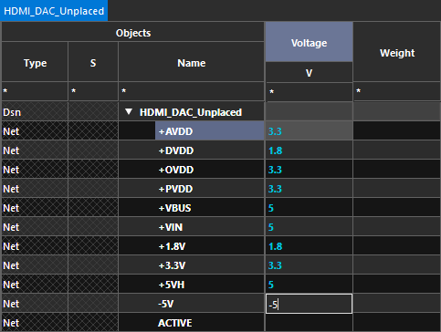
Step 41: All nets in the design are listed with their properties such as voltage, weight, and routing priority. Enter voltages for the following nets:
- +AVDD: 3.3
- +DVDD: 1.8
- +OVDD: 3.3
- +PVDD: 3.3
- +VBUS: 5
- +VIN: 5
- +5VH: 5
- -5V: -5
Step 42: Scroll down to net 0 (ground) and enter 0 for the voltage.
Step 43: Close the Constraint Manager.
Step 44: Select File > Save from the menu to save the board file. Click Yes if prompted to overwrite.
Importing the Design into X AI
Step 45: With rooms and constraints configured, the board can be imported into X AI. Select Tools > X AI from the menu.
Step 46: Select Login and enter your Cadence username and password.
Step 47: Select Create New Workspace at the top of the Workspaces panel.
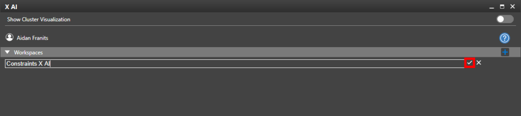
Step 48: Enter a name for the new workspace and click the checkmark button to create it.
Step 49: In the main workspace window, select Upload Board to upload the currently-loaded board to the X AI server.
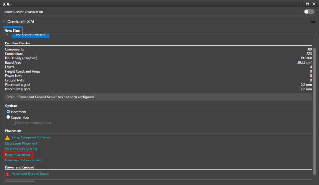
Step 50: To view the rooms defined earlier, select Room Placement in the X AI window.
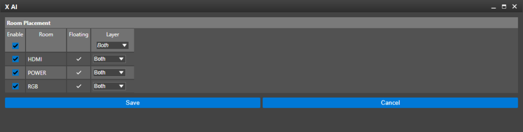
Step 51: The Room Placement table opens. The HDMI, RGB, and Power rooms are listed as defined. Click Save or Cancel to return to the main window.
Step 52: To view power and ground net voltage assignments, select Power and Ground Setup.
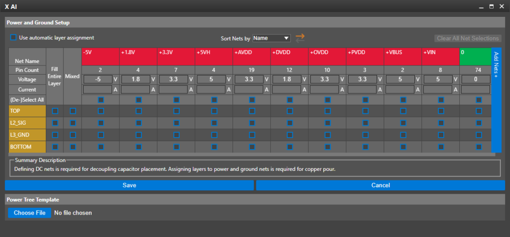
Step 53: The Power and Ground Setup table opens. The top row shows the defined power and ground nets with their number of connections and assigned voltages below.
The board is ready to leverage Allegro X AI for AI-generated component placement and copper pours.
Note: Depending on the board, additional settings may need to be configured in the X AI window. To learn how to configure X AI-specific settings, see our how-to here.
Wrap Up & Next Steps
Quickly and easily configure constraints and design settings including rooms, physical rules, spacing rules, voltages and more to ensure AI will return results that meet your design and functionality criteria with Allegro X AI in OrCAD X. Test this feature and more with a free trial of OrCAD. Get more how-tos for OrCAD at EMA Academy.

