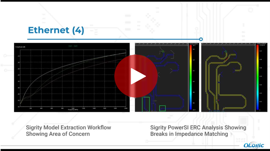
While IoT devices may seem simple to the end users (which is good), the electrical design complexity of these devices is often very high. Designers are required to work with limited board space while functionality and speed requirements continue to increase. These tight spaces, combined with the required highspeed signaling, leads to increased susceptibility to SI/PI/EMI/RF issues. This makes time-to-market, cost, and manufacturing requirements a significant challenge to meet. While these challenges are not going to get any easier, there are solutions that enable designers to confidently deliver these complex products on-time and on budget. Learn from the experts at Cadence and EMA how the Intelligent System Design platform at the heart of the Cadence PCB flow enables teams to concurrently manage and overcome these challenges early in the design process, optimize the design, and verify functionality for first pass success.