

When designing a PCB, one of the more important steps for routing and integrity analysis is configuring power net voltages. While these voltages can be defined in the PCB stage, voltages can be assigned during schematic creation to ensure design intent is retained throughout the entire design. With OrCAD X Capture easily assign voltage values to DC nets during schematic creation to ensure clarity throughout the design process.
This quick how-to will provide step-by-step instructions on how to assign voltage values to DC nets during schematic creation in OrCAD X Capture.
To follow along, download the provided files above the table of contents.
How-To Video
 Open in New Window
Placing Power
Step 1: Open the provided design in OrCAD X Capture.
Step 2: To place power in the schematic, select Place > Power from the menu.
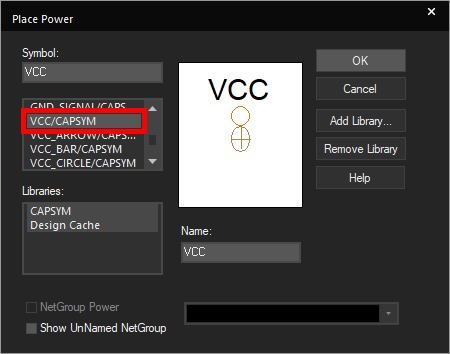
Step 3: In the Place Power window, scroll down and select VCC/CAPSYM for the power marker and click OK to attach it to your cursor.
Step 4: To set the net name, right-click and select Edit Properties.
Step 5: Enter +5V for the name and click OK.
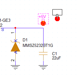
Step 6: Click to place the power symbol at the 5V rectifier output.
Step 7: Right-click and select Edit Properties. Enter +3V3 for the name and click OK to place the 3.3V marker.
Step 8: Click to place the marker at the 3.3V rectifier output.
Step 9: Right-click and select Edit Properties. Enter +AVCC for the name and click OK.
Step 10: Click to place the marker at the AVCC rectifier output.
Step 11: Right-click and select Edit Properties. Enter +BL for the name and click OK.
Step 12: Click to place the marker at the BL rectifier output.
Step 13: Right-click and select Edit Properties. Enter -7V for the name and click OK.
Step 14: Click to place the marker at the -7V rectifier output.
Step 15: Right-click and select Edit Properties. Enter +12V for the name and click OK.
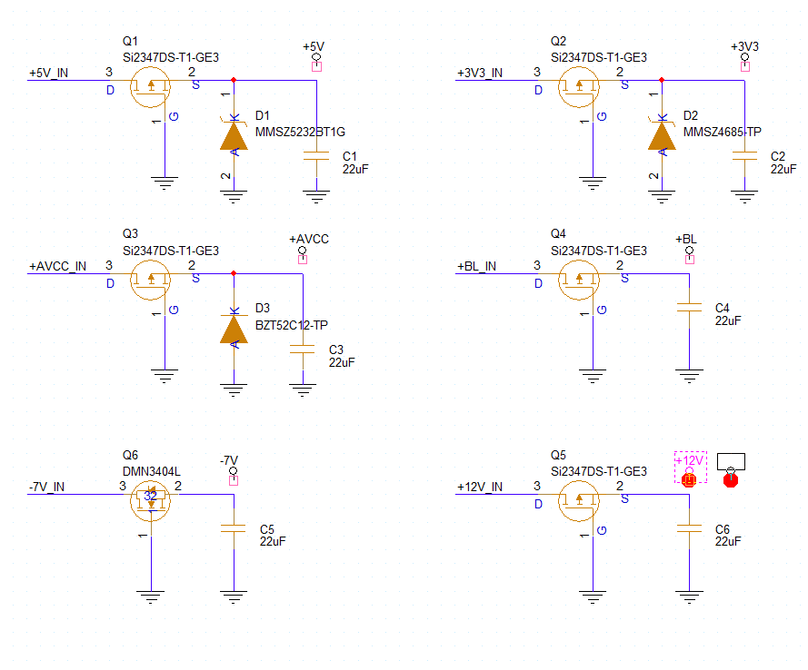
Step 16: Click to place the marker at the 12V rectifier output. The DC nets have been aliased. Right-click and select End Mode.
Establishing Power Connections in the Schematic
Step 17: To connect power to the rectifier outputs, select Place > Wire from the menu.
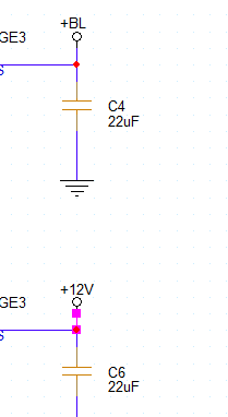
Step 18: Click to draw a wire between each rectifier output and marker. When finished, press Escape on the keyboard.
Assign Voltage Values to DC Nets
Step 19: DC nets can be identified through SI analysis in OrCAD X Capture. To activate SI analysis, select the design file in the Project Manager.
Step 20: Select SI Analysis > Identify DC Nets from the menu.
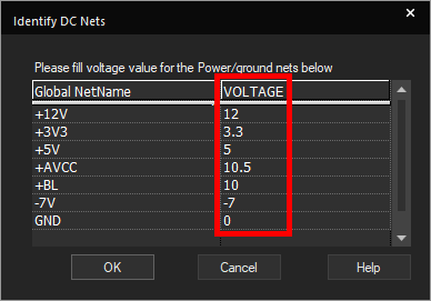
Step 21: The Identify DC Nets window opens, showing a table to define the voltage for each global net. Enter the following voltage values:
- +12V: 12
- +3V3: 3.3
- +5V: 5
- +AVCC: 10.5
- +BL: 10
- -7V: -7
- GND: 0
Step 22: Click OK to assign the voltages.
Viewing Net Voltages
Step 23: Voltages can be viewed in the Net properties table. Right-click the design file in the Project Manager and select Edit Object Properties.
Step 24: The Property Editor tab opens. Select the Flat Nets tab. Voltages are listed in the bottom row for the relevant nets.
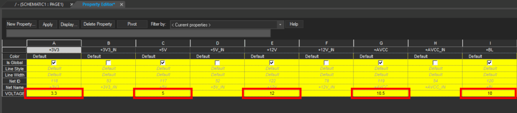
Step 25: Close the Property Editor tab when finished. Voltages are now associated with nets and will be transferred to the PCB layout.
Wrap Up & Next Steps
Quickly assign voltage values to DC nets in the schematic canvas to ensure design intent remains apparent in all stages of the design process in OrCAD X Capture. Test this feature and more with a free trial of OrCAD X. Want to learn more about Capture? Get access to free how-tos, courses, and walk-throughs at EMA Academy.

