

Ultra Librarian, SamacSys, and other sources provide a wide variety of verified PCB footprints for quick and efficient design creation; however, sometimes a symbol and footprint will need to be created manually. While many templates exist for footprint creation, the correct model may not be available especially for specialty components like circular connectors. Quickly create a PCB footprint for circular connectors and other components with OrCAD X using either Cartesian and polar systems.
This quick how-to will provide step-by-step instructions on how to create a PCB footprint for circular connectors and other complex components with the Footprint Editor in OrCAD X.
To follow along, download the provided files above the table of contents.
How-To Video
 Open in New Window
Create a PCB Footprint
Step 1: Open OrCAD X.
Step 2: To create a PCB footprint in OrCAD X, select File > New > Footprint from the menu to create a new footprint.
Step 3: A footprint file is created in your home directory. To save the file in your working directory, select File > Save As from the menu.
Step 4: Browse to the working directory. Enter 1551422.dra for the file name and click Save. The drawing is saved in the working directory.
Defining Design Units
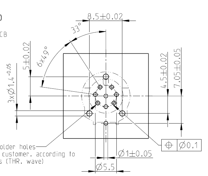
Step 5: Open the provided 155422_Rev_B_Dwg.pdf file in your preferred PDF viewer. Zoom into the dimensioned drawing of the connector. This datasheet gives dimensions in millimeters, so the units in OrCAD X must be adjusted accordingly.
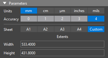
Step 6: In OrCAD X, in the Properties panel, under Parameters, select mm for the units. The accuracy automatically changes to 4 decimal places.
Create a PCB Footprint: Center Pin
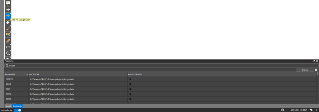
Step 7: Select Add Pin using Search from the toolbar. The Padstacks panel opens with a list of available padstacks to be placed.
Step 8: Select Browse. Browse to the working directory and select the provided pad60cir20d.pad padstack file.
Note: To learn more about how to create a padstack to use in your own designs, see our how-to here.
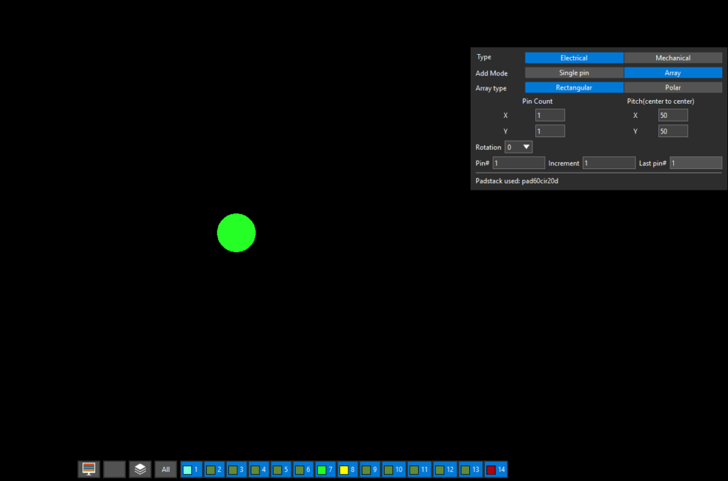
Step 9: The padstack is attached to your cursor. Click to place the padstack at the design origin. This pin will act as the center pin #8 in the connector. Scroll the mouse wheel up to zoom in as needed.
Create a PCB Footprint: Radial Pins
Step 10: In the pin placement widget, select Polar for the Array Type.
Step 11: Set the Angle Increment to 49.
Step 12: Select Grids to open the Grid subpanel.
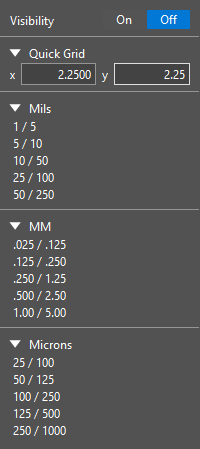
Step 13: Enter 2.25 into each Quick Grid field for a snap of 2.25mm.
Note: As shown in the datasheet, the diameter of the pin circle is 5.5mm. This will allow a pin to be placed at the radius, 2.25mm from the origin/center.
Step 14: Select the origin to define the center of the pin circle. A pin is attached to your cursor.
Step 15: Move your mouse below the center pin. The new pin snaps to the radius of 2.25mm. Click to place another pin.
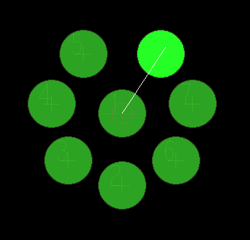
Step 16: Click to place six additional pins around the pin circle as shown in the datasheet. The new pins snap to the 49° increment automatically. Press Escape when finished.
Create a PCB Footprint: Non-Plated Holes
Step 17: Select Add Pin Using Search again to open the Padstacks panel.
Step 18: Click Browse. Browse to and select the provided hole55.pad file. This is an unplated mechanical hole.
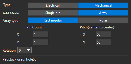
Step 19: In the pin placement widget, select Mechanical for the Type and Rectangular for the Array Type.
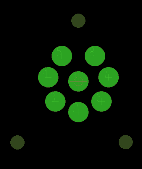
Step 20: Click to place three mechanical holes in the approximate locations given by the datasheet.
Step 21: Select the Move mode from the toolbar.
Step 22: Select the uppermost mechanical hole to attach it to your cursor.

Step 23: Press Tab to set the coordinates to move the hole to. Enter 0 for the X coordinate. Press Tab again and enter 5 for the Y coordinate. Press Enter to set the hole position.
Step 24: Select the lower left mechanical hole and press Tab. Enter -4.25 for the X coordinate and -4.5 for the Y coordinate.
Step 25: Select the lower right mechanical hole and press Tab. Enter 4.25 for the X coordinate and -4.5 for the Y coordinate.
Step 26: Select Add Pin Using Search again to open the Padstacks panel. Click Browse. Browse to and select the provided hole40.pad file.
Step 27: Click to place the lowest mechanical hole as per the datasheet.
Step 28: Select the Move mode again and click the new hole.
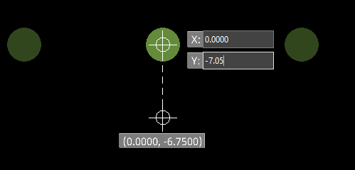
Step 29: Press Tab to set the coordinates. Enter 0 for the X coordinate and -7.05 for the Y coordinate.
Create a PCB Footprint: Silkscreen
Step 30: Select the Create Shape mode from the toolbar.
Step 31: The Create Shape widget opens. Select Circle for the shape type.
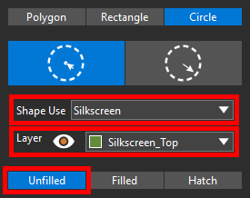
Step 32: Select Silkscreen from the Shape Use dropdown and Silkscreen_Top from the Layer dropdown. Select Unfilled to create an unfilled shape.
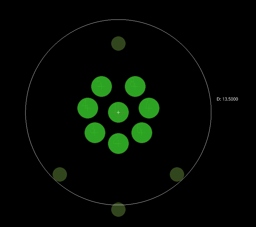
Step 33: Select the origin to define the center of the circle. The circle outline is attached to your cursor. Move the mouse until the diameter reads approximately 13.5mm and click again to place the circle.
Note: If needed, disable All Objects in the Selection Filter to prevent pins and text from being selected.
Step 34: Select Rectangle from the Create Shape widget.
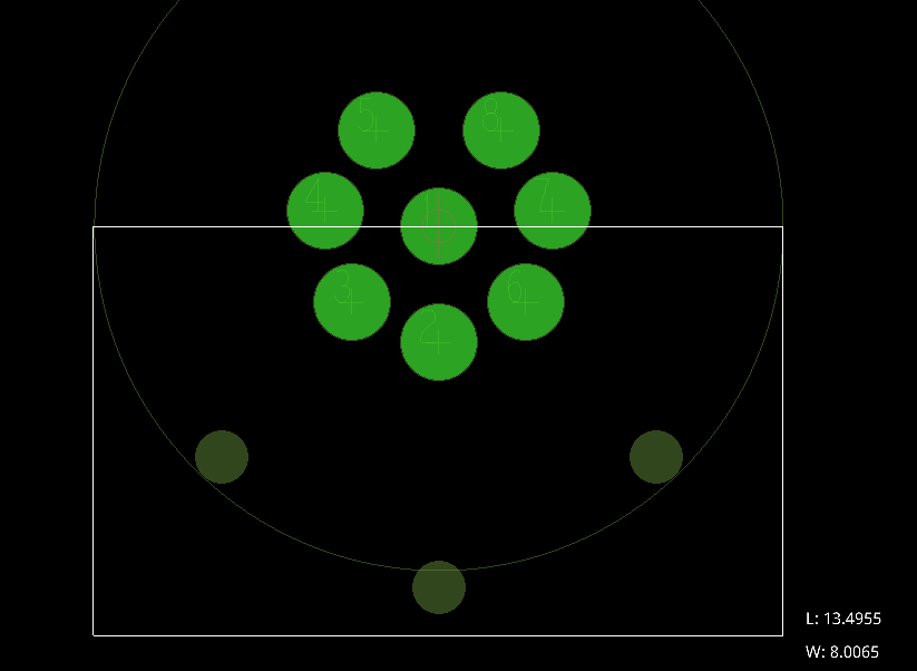
Step 35: Click the leftmost point of the circle to start drawing the rectangle. Draw the rectangle to the width of the circle and down approximately 8mm and click again to place. A crosshair symbol appears when a shape corner can be snapped to the feature under your cursor.
Step 36: Choose the Select mode from the toolbar or press Escape on the keyboard.
Step 37: Click and drag to adjust the rectangle to snap the right side to the rightmost point of the circle.
Step 38: Select Add Refdes from the toolbar.
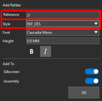
Step 39: In the Add Refdes widget, enter J? For the reference and set the style to REF_DES.
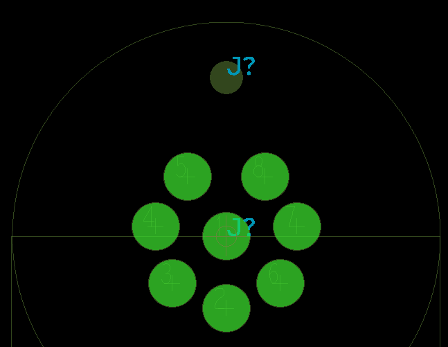
Step 40: Click OK to create the reference designator. The reference designator is automatically placed at the top of the footprint. When the footprint is used in a design, the reference designator is automatically changed to that of the linked component.
Step 41: Select File > Save from the menu to save the footprint.
Wrap Up & Next Steps
Quickly and easily create a PCB footprint for a circular connector and other complex components in OrCAD X. Test this feature and more with a free trial of OrCAD X. Get more how-tos for OrCAD X at EMA Academy.

