With today’s ever-increasing design complexity, multiple-pin connections between boards is inevitable. Projects often have two or more PCBs in the same enclosure that must communicate with each other and keeping track of connector pinouts between boards or components is critical to ensure proper functionality. The Multi-Board Connector Pin Check App included with the EMA Toolkit will check the pin-out of mating connectors between two schematics to quickly identify any inconsistencies.
This quick how-to will provide step-by-step instructions on how to check the pinout of mating connectors between two schematics with the Multi-Board Connector Pin Check app in OrCAD Capture.
To follow along, download the provided files above the table of contents.
How-To Video
 Open in New Window
Check the Pin-Out of Mating Connectors
Step 1: Open the provided design, pin_connect.dsn, in OrCAD Capture.
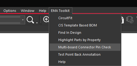
Step 2: Select EMA Toolkit > Multi-board Connector Pin Check from the menu. The Connector Pin Connectivity window will open. Pin_connect.dsn will be automatically assigned as Design 1.
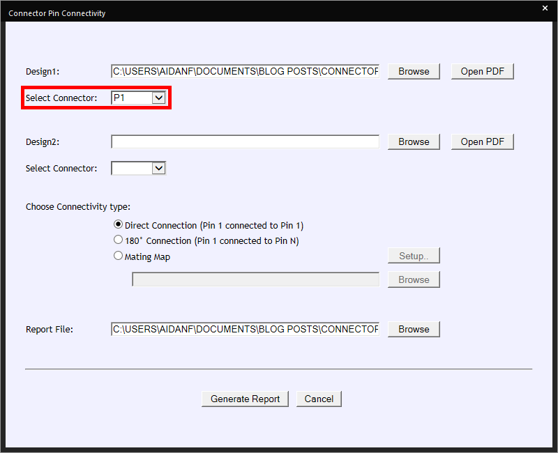
Step 3: Ensure that the Select Connector option for Design 1 is set to P1.
Note: This dropdown lists all connectors in the design. In this case, all components whose reference designators start with J or P.
Step 4: Select Browse for Design 2.
Step 5: Select Pin_Connect2.dsn from the downloaded files and click Open.
Step 6: Ensure that the Select Connector option for Design 2 is set to J1.
Step 7: Ensure the option for Choose Connectivity Type is set to Direct Connection.
Note: This defines how the pins are supposed to be connected.
- Direct Connection: All pin numbers are the same between the two connectors.
- 180° Connection: Pin numbers are reversed between the two connectors. For example, with an 8-pin connector, pin 1 connects to pin 8.
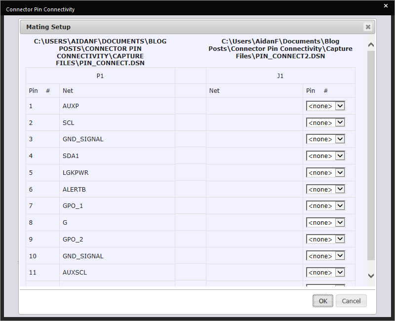
- Mating Map: Pin mapping is defined in the Mating Setup panel or through an external file.
Step 8: Select Generate Report to create the report.
Identifying and Correcting Mismatched Pins
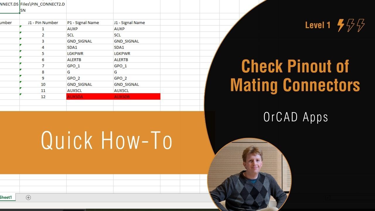
Step 9: By default, the report is saved as PIN_CONNECT_Connectivity.xlsx in the Design 1 folder. Open the file in Microsoft Excel if it does not open automatically.
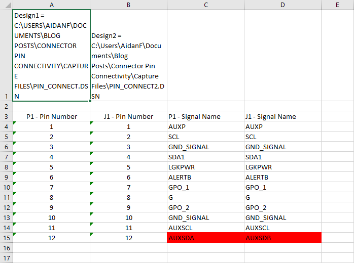
Step 10: View the report. Pin 12 on both P1 and J1 is highlighted in red, indicating that the signal names do not match.
Step 11: Close the report file. Back in Capture, select File > Open > Design from the menu.
Step 12: Browse to the location of design Pin_Connect2.dsn. Select the file and click Open.
Step 13: Since there is no project file associated with this design, the Select Project Type window opens. Leave the default settings and click OK.
Step 14: Double-click .\pin_connect2.dsn > SCHEMATIC1 > PAGE1 from the design hierarchy.
Step 15: Double-click the net alias AUXSDB to open the Edit Net Alias window.
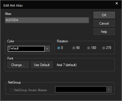
Step 16: Rename the net SDA and click OK.
Step 17: Select File > Save from the menu. Close the PIN_CONNECT2.opj project.
Step 18: Select EMA Toolkit > Multi-board Connector Pin Check from the menu.
Step 19: Select Browse for Design 2. Select Pin_Connect2.dsn from the downloaded files and click Open.
Step 20: Select Generate Report. Click Yes when prompted to overwrite the xlsx file.
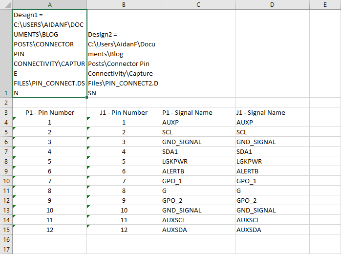
Step 21: Open the file in Microsoft Excel if it does not open automatically. None of the cells are highlighted in red, indicating that all net names and pins match.
Wrap Up and Next Steps
Quickly and easily check the pin-out of mating connectors between two schematics with the Multi-Board Connector Pin Check App in OrCAD Capture. This app and others are part of the EMA Toolkit, one of the benefits of EMA Support +. The EMA Support + program is available to all EMA customers on active support and includes additional benefits and tools to expedite the PCB design process, such as time saving apps, additional training, and more. See what’s included with EMA Support + and learn how to get access to these exclusive benefits.

