Today, successful designs typically go through multiple revisions in order to:
- Reduce costs and improve profits
- Replace obsolete or unavailable components
- Improve speed and performance
- Address new market demands
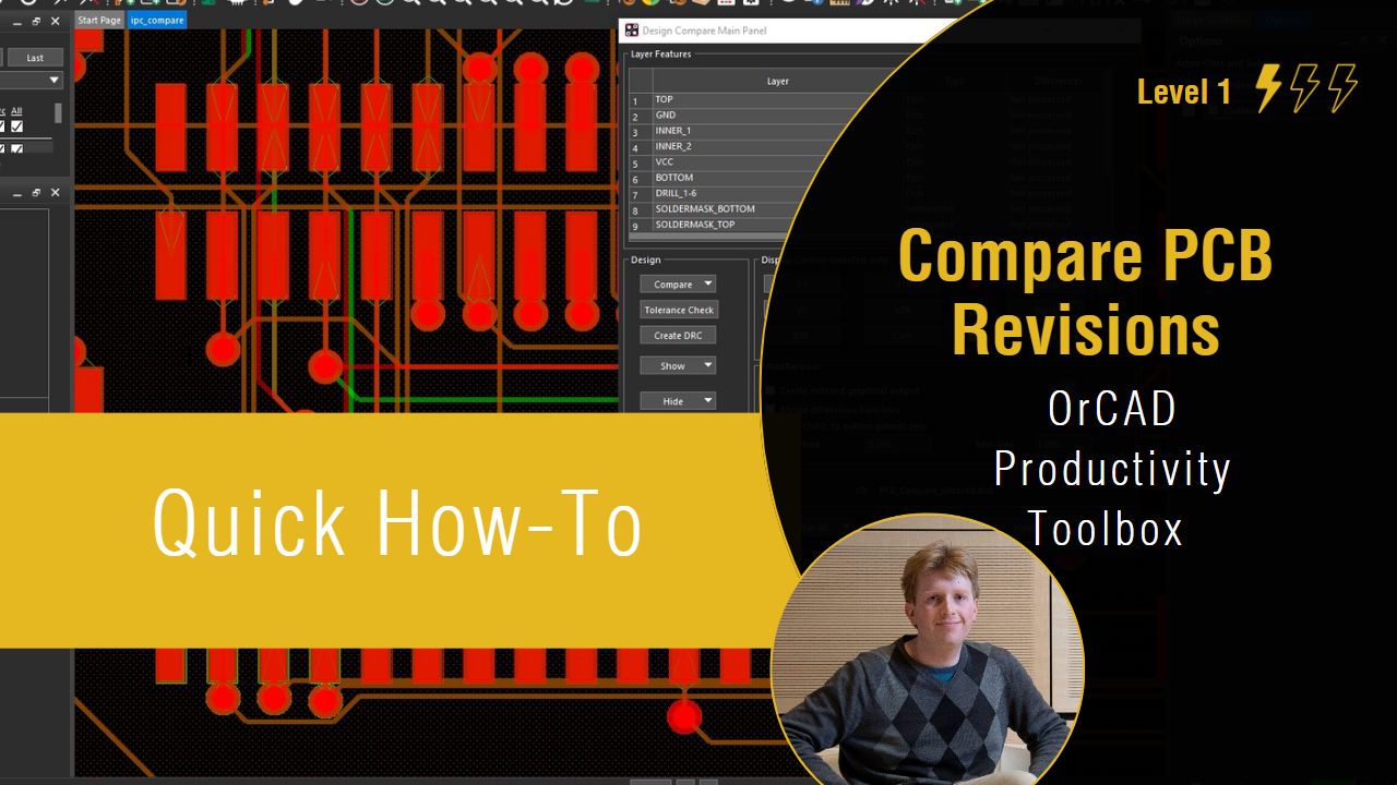
Keeping track of these changes to the board and product lifecycle is critical; however, relying on notes and manual methods for change identification and tracking is error-prone and timely. Quickly compare PCB designs and find differences between revisions with PCB Compare in OrCAD Productivity Toolbox. PCB Compare allows you to:
- Print differences between boards in an HTML document
- View differences visually on the PCB canvas
This quick how-to will provide step-by-step instructions for using PCB Compare in OrCAD PCB Designer to automatically identify and review chances between PCB revisions.
To follow along, use the provided designs above the table of contents.
How-To Video
Performing a Textual (Standard) Comparison
Step 1: Open the provided design, PCB_Compare_Unglossed.brd,in OrCAD PCB Designer Professional with the OrCAD Productivity Toolbox option selected.
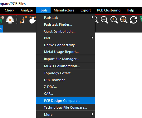
Step 2: Select Tools > PCB Design Compare from the menu.
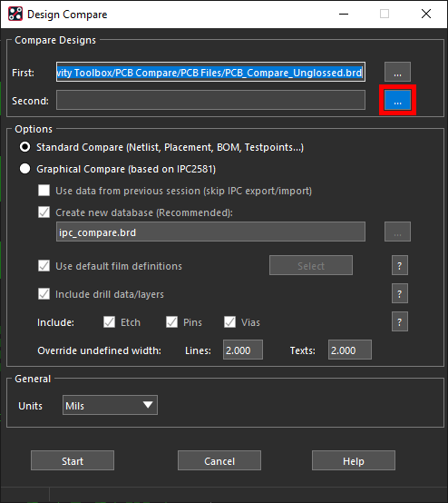
Step 3: The open design is automatically selected as the first design to compare. Select the ellipsis to load the second design.
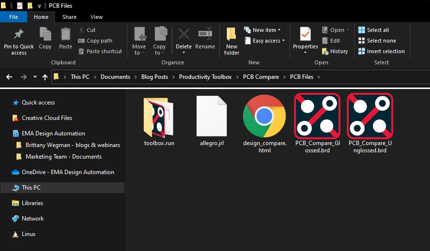
Step 4: Browse to the provided design, PCB_Compare_Glossed.brd. Select the design and click Open.
Note: If desired, change the design units with the Units dropdown.
Step 5: Select Start to run the analysis.
Step 6: The comparison file is saved as design_compare.html. Open the file in your preferred Web browser.
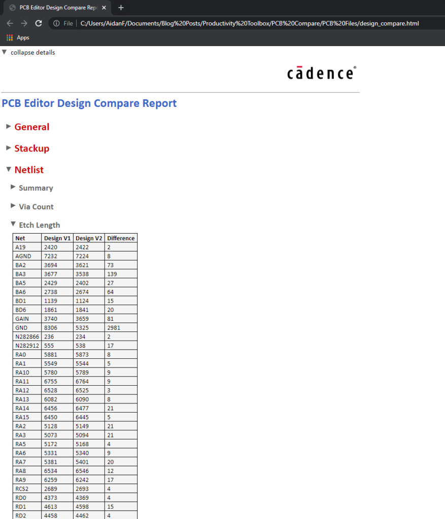
Step 7: View the comparison data. Expand Netlist > Etch Length to see the different etch lengths between the two boards.
Note: A Standard Comparison Report contains design differences for:
- Modification of stackup
- Netlist and connectivity
- Pin connectivity modifications
- Property changes
- Test point modifications (moved, renamed, etc.)
- Devicetype modifications (ECO part)
- Placement modifications
- Renamed components
Performing a Graphical Comparison
Step 8: A graphical compare will show the differences between the two boards visually. Back in PCB Designer, select Tools > PCB Design Compare from the menu.
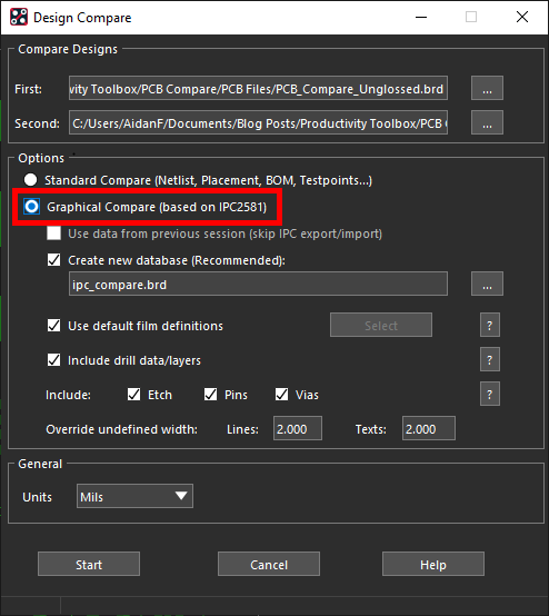
Step 9: Select the Graphical Compare radio button.
Note: The first and second designs to compare are retained from the previous use of the comparison tool.
Step 10: Leave the settings as the default and select Start to run the comparison. The ipc_compare.brd file is created and opened automatically.
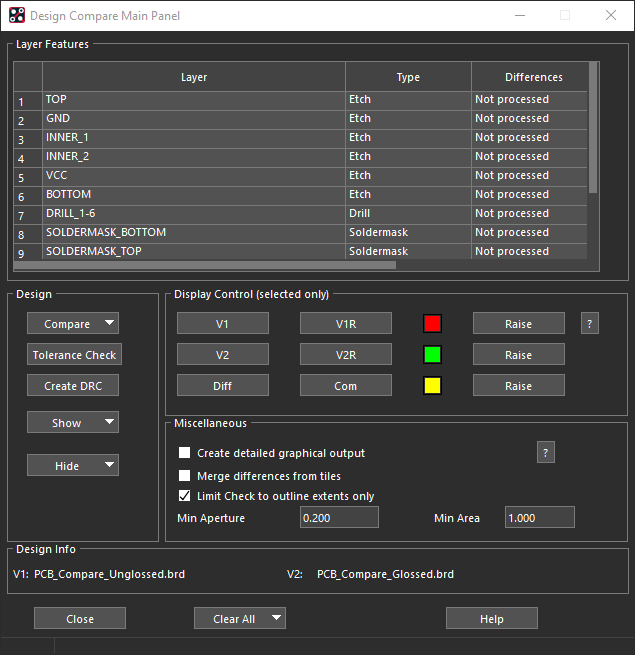
Step 11: When the comparison finishes, the Design Compare Main Panel window opens. This window lists the differences between layers and the colors used for each design.
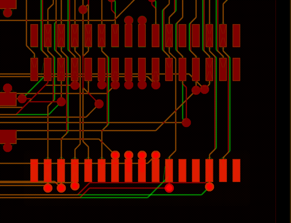
Step 12: Zoom into the component pins on the PCB. Red traces are part of the original unglossed design, while green traces are part of the glossed design. Orange-brown traces are part of both.
Wrap Up & Next Steps
Quickly compare PCB design revisions and efficiently identify changes with PCB Compare in OrCAD Productivity Toolbox. To learn more about how the features of OrCAD Productivity Toolbox can expedite your PCB designs, view our latest webinar.

