During the design review process, optimizing the PCB layout and verifying that all aspects are up-to-date is critical to streamline manufacturing and reduce costs. Something as small as an incorrect padstack or out-of-date drill chart can result in unintended manufacturing consequences. One way to improve the manufacturing process is to review drill holes in the design to:
- Verify the correct padstack is used
- Ensure conformity to the manufacturer’s equipment and tolerances
- Minimize the number of different drill sizes used
Easily find padstacks used in the design to quickly review the type and quantity with the Padstack Finder in OrCAD Productivity Toolbox. With the Padstack Finder, users can:
- Search by padstack name
- Search by drill size
- Distinguish between pins, vias, and stacked vias
- Highlight and cross-probe with the PCB canvas
This quick how-to will provide step-by-step instructions to efficiently find padstacks in the PCB design with the Padstack Finder in OrCAD PCB Designer.
To follow along, download the provided files above the table of contents.
How-To Video
Find Through-Hole Padstacks
Step 1: Open the provided design in OrCAD PCB Designer Professional with the OrCAD Productivity Toolbox option selected.
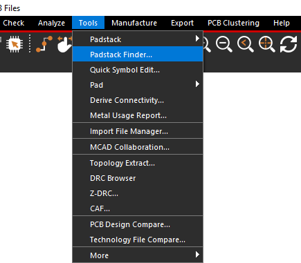
Step 2: Select Tools > Padstack Finder from the menu to open the Padstack Finder window.
Note: The Padstack Finder window has options to filter the list of padstacks by:
- Object type: pins, vias, or stacked vias
- Pattern
- Drill size
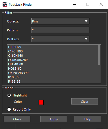
Step 3: Select C140_H90 from the list to find this through-hole padstack.
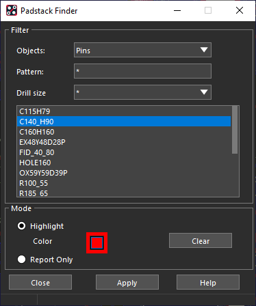
Step 4: Under Mode, be sure Highlight is selected. Select the color to change it.
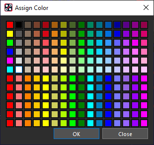
Step 5: Select a color, e.g. white, from the Assign Color window.
Step 6: Select Apply in the Padstack Finder.
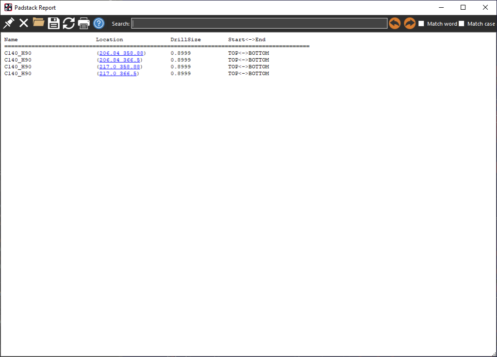
Step 7: The Padstack Report window opens. View and close the report.
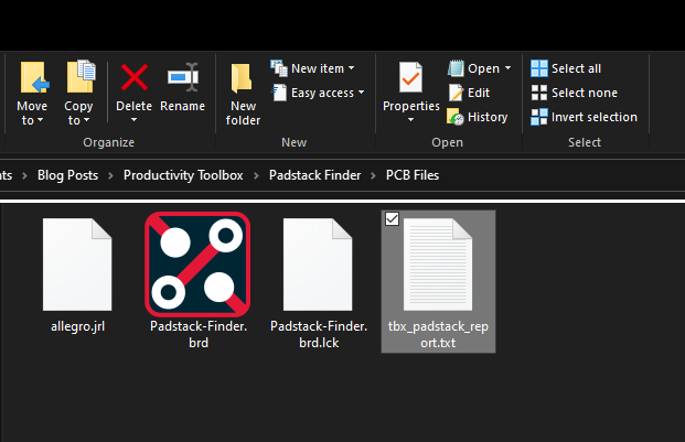
Note: The most recent report is saved in the working directory. The Padstack Report shows:
- The locations of all instances of this padstack
- The drill size
- The starting and ending layers
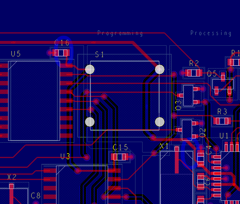
Step 8: Minimize the Padstack Finder. The padstacks are highlighted in white in the PCB canvas.
Find Padstacks by Name
Step 9: Back in the Padstack finder, select Clear to clear the highlights.
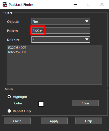
Step 10: Enter RX22Y* into the Pattern field and press Tab on the keyboard.
Note: Adding an asterisk to the end of the search will return any padstacks with the same beginning criteria. In this example, the padstack list is filtered to padstacks starting with “RX22Y.”
Step 11: Select padstack RX22Y34D0T and click Apply.
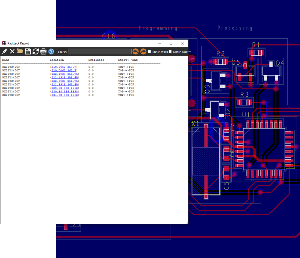
Step 12: The Padstack Report opens and the padstacks are highlighted on three transistors in the design.
Note: Since this is a surface-mount padstack, the drill size is now listed as 0 and the starting and ending layers are the same.
Step 13: Close the Padstack Report.
Step 14: Select RX22Y52D0T from the padstack list and click Apply.

Note: A new report opens and new highlights are drawn but none of the existing highlights are cleared.
Step 15: Select Clear to clear the highlights.
Find Padstacks by Drill Size
Step 16: Replace the text in the pattern field with an asterisk (*).
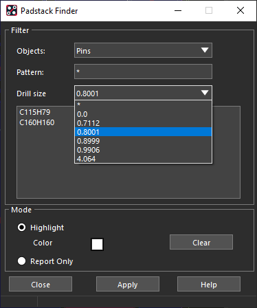
Step 17: Select 0.8001 from the Drill Size drop-down menu. The padstack list is filtered to padstacks with a drill size of 0.8001mm.
Step 18: Hold Shift and select both C115H79 and C160H160. Select Apply.
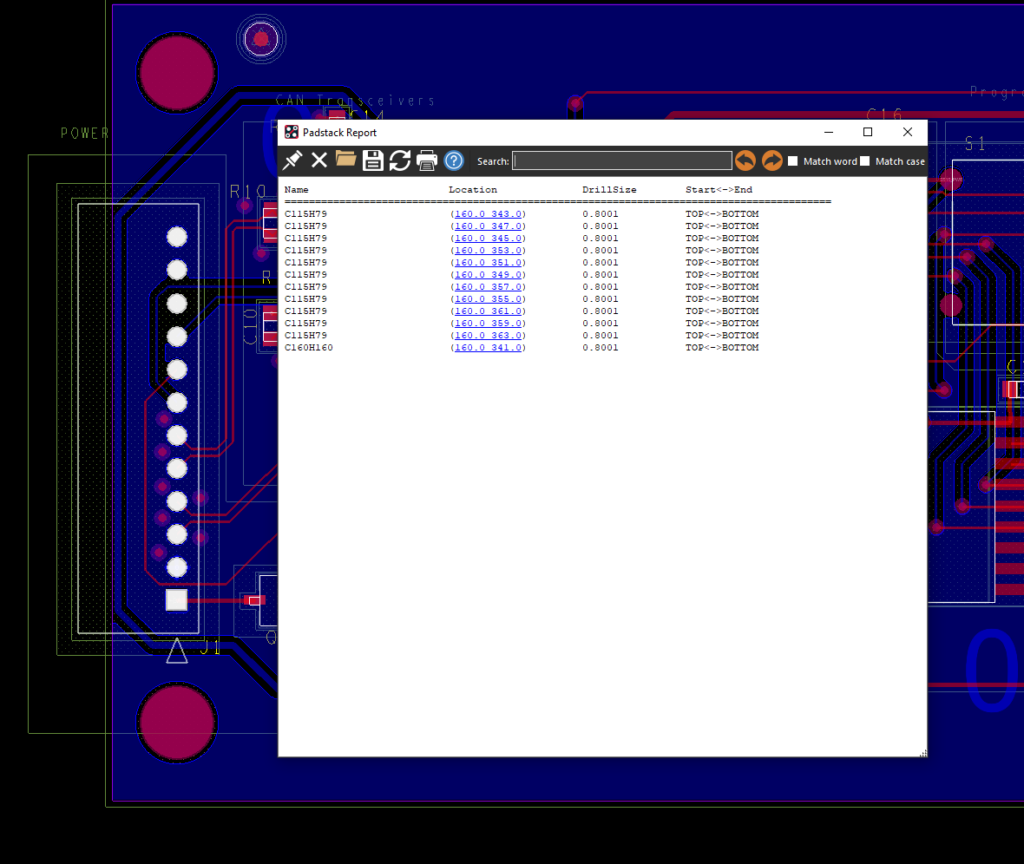
Step 19: All pads in connector J1 are highlighted. Select Clear and Close to close the Padstack Finder.
Wrap-Up & Next Steps
Quickly find padstacks with efficient identification of the type and quantity used in your PCB and accelerate the design review process with the Padstack Finder in OrCAD Productivity Toolbox. To learn more about how the features of OrCAD Productivity Toolbox can expedite your PCB designs, view our latest webinar.

