

When a trace segment crosses a split plane, gap or void in a reference plane, it can create issues with signal integrity, EMC and reliability. These can include:
- Return current disruption
- Increased EMI/EMC radiation
- Impedance discontinuities which cause signal integrity degradation
- Increased crosstalk
With dense, complex boards consisting of multiple layers, these issues can be hard to identify. Easily detect trace segments over voids with OrCAD X to improve design performance throughout the PCB layout process.
This quick how-to will provide step-by-step instructions on how to detect trace segments over voids in OrCAD X to reduce impedance discontinuities and return path disruptions, improving signal and power integrity.
To follow along, download the provided files above the table of contents.
How-To Video
 Open in New Window
Detect Trace Segments Over Voids
Step 1: Open the provided design in OrCAD X.
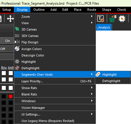
Step 2: To highlight the trace segments that pass over voids, select Display > Segments Over Voids > Highlight from the menu.
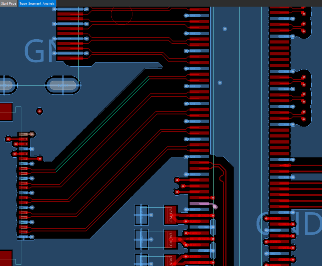
Step 3: View the PCB canvas. Trace segments that pass over voids, which could potentially cause signal integrity and power integrity issues is highlighted.
Analyzing Trace Segments Over Voids
Step 4: A log file opens, showing a list of segments routed over voids and segments with missing plane coverage. Select the coordinates for CAM1_DP3 to be brought to the location of the offending void.
Step 5: Since the affected trace is on the TOP layer, the return path void must be on the GNDT layer below it. Check the box under All for GNDT in the Visibility panel.
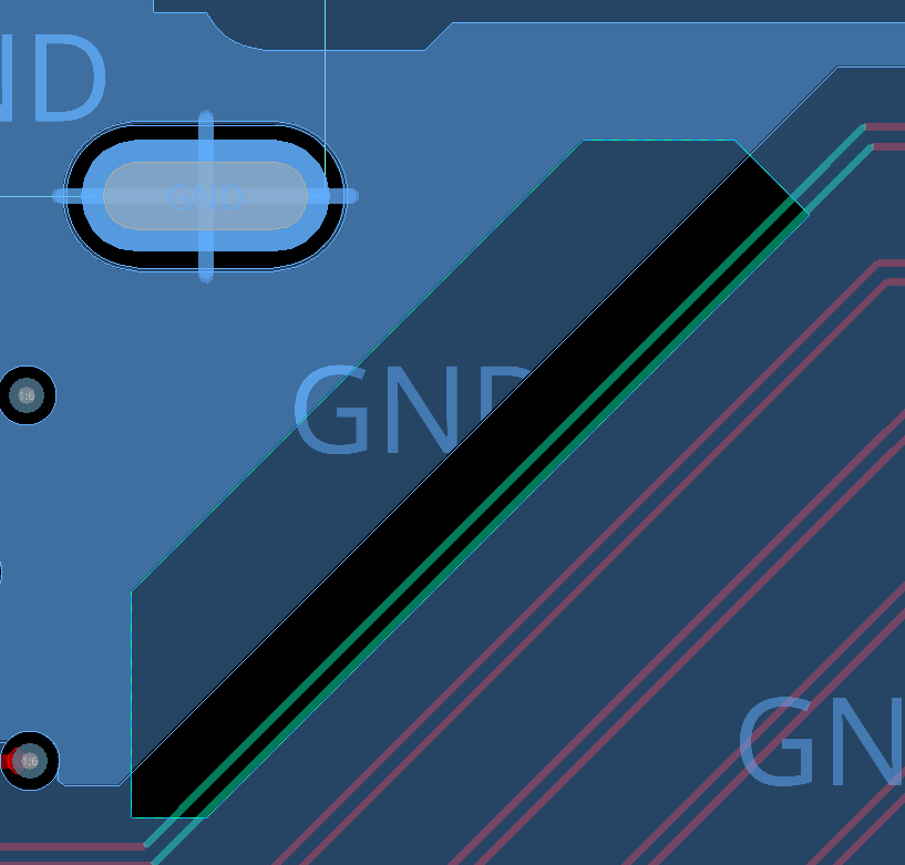
Step 6: View the board. A void in the top ground plane under the uppermost CAM1 net is clearly visible.
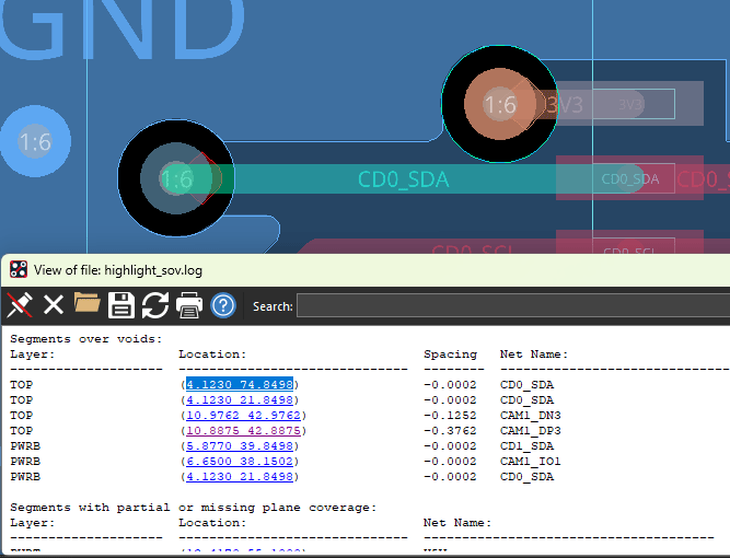
Step 7: Back in the highlight log, select the location for the first instance of the CD0_SDA net on the TOP layer. The void here is created by the via on the 3V3 net. The trace only partially covers the void, as shown by the spacing of 0.0002mm.
Step 8: Close the log window.
Correcting Trace Segments Over Voids
Step 9: Select Display > Segments Over Voids > Dehighlight from the menu. The highlighting is removed.
Step 10: To correct the issue traces can be moved out of the way. Select the Slide mode from the toolbar.
Step 11: In the Options panel, set the Bubble mode to Shove Preferred to move other traces as required.
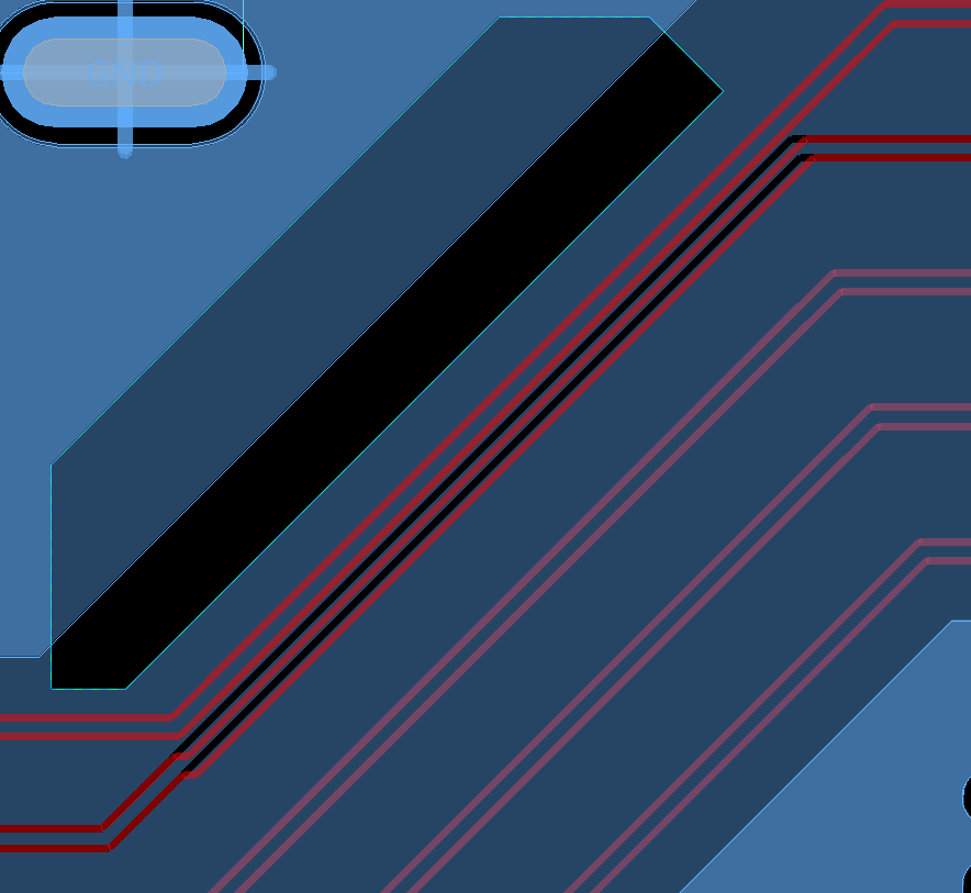
Step 12: Select the uppermost traces. Move the traces to be out of the way of the void and click again to place.
Note: Differential traces are adjusted in pairs. If you get too close to other traces, they are pushed further down.
Step 13: Scroll up to zoom into the via on the 3V3 net that created the small void.

Step 14: Click the via to adjust its position. Move the via to be farther away from the trace and click again to place it. Right-click and select Done.
Verifying Trace Corrections
Step 15: To check the segments again, select Display > Segments Over Voids > Highlight from the menu.
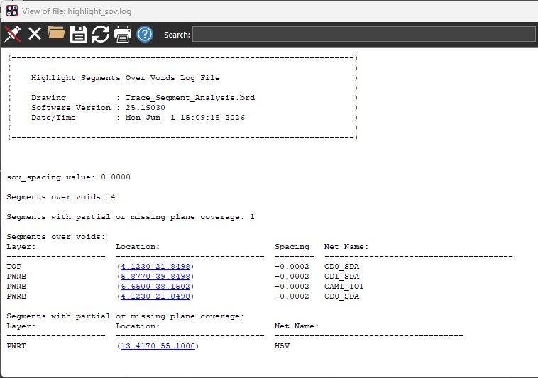
Step 16: View the log file. Only a few traces with segments over voids remain, all with spacing of less than a micrometer. Complete this process as required for the design.
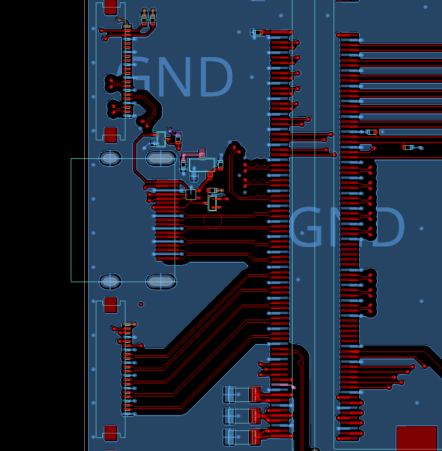
Step 17: Close the log file and view the board. Uncheck All for GNDT in the Visibility panel for better visibility of the TOP layer. The previously-highlighted traces are no longer highlighted, indicating that there are no longer trace segments crossing voids.
Note: Additionally, impedance analysis can be performed directly in the PCB canvas to detect impedance discontinuities, such as segments over voids, with color-coded overlays for easy identification. Get step-by-step instructions here.
Wrap Up & Next Steps
Quickly and easily detect trace segments over voids to identify potential signal integrity and power integrity issues during PCB layout with OrCAD X. Test this feature and more with a free trial of OrCAD X. Get more how-tos for OrCAD at EMA Academy.

