Although digital circuitry has become ubiquitous in modern electronics, for circuits such as audio amplifiers and power supplies, thorough analog circuit analysis is still a must. Analog analysis may even be run on digital circuitry to ensure that the noise is acceptable. In some cases, it may be necessary to simulate and adjust the desired impedance for a circuit before the circuit map itself is known. PSpice Designer allows you to quickly and easily model impedance or admittance to expedite the design and testing processes with analog behavioral models. To model impedance in PSpice, analog behavioral models (ABMs) are used to define sets of electronic components mathematically, for example, to model a large number of components in a single package.
This quick how-to will provide step-by-step instructions on how to model impedance in PSpice with analog behavioral models (ABMs).
How-To Video
 Open in New Window
Model Impedance in PSpice: Linear Impedance
Step 1: Open PSpice Designer.
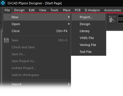
Step 2: Select File > New > Project from the menu.
Step 3: The New Project window opens. Enter the name ABM_Impedance. Select the ellipsis under Location and browse to the working directory. Ensure Enable PSpice Simulation is checked and click OK.
Step 4: The Create PSpice Project window opens. Select Create a Blank Project and click OK.
Step 5: The schematic canvas opens. Select Place > Component from the menu to open the Component Explorer tab.
Step 6: In the Categories list, expand PSpice > Source > Controlled Sources and select Current Source.
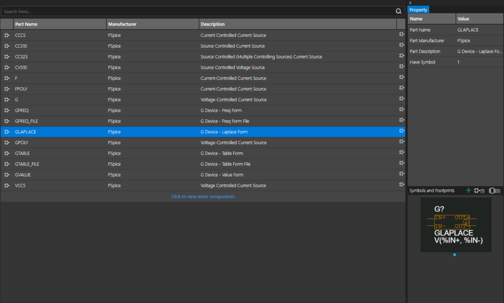
Step 7: Select GLAPLACE from the list to place a Laplace-dependent voltage-controlled current source. Double-click to attach the model to your cursor.
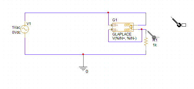
Note: Impedance can act like a voltage-controlled current source. The current between its output nodes is a Laplace function times the voltage across its input nodes. If the input and output nodes are connected, the source acts as a behavioral model of a resistive or reactive circuit.
Step 8: Click to place the model in the schematic, then right-click and select End Mode.
Creating a Test Circuit
Step 9: To power the behavioral model, select Place > PSpice Part > Source > Voltage Sources > DC from the menu.
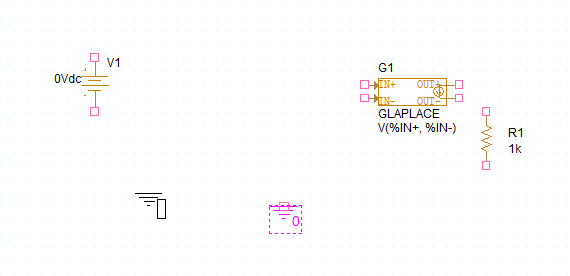
Step 10: Click to place a voltage source in the schematic. Right-click and select End Mode.
Step 11: Select Place > PSpice Part > Resistor from the menu.
Step 12: Click to place the resistor as a circuit load. Right-click and select End Mode.
Note: Press R on the keyboard to rotate the component as required.
Step 13: A PSpice ground object is required for simulation. Select Place > PSpice Part > PSpice Ground from the menu.
Step 14: Click to place the ground at the bottom of the circuit. Right-click and select End Mode.
Step 15: Select Place > Wire from the menu, the Wire button from the toolbar, or press W on the keyboard.
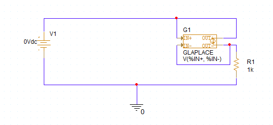
Step 16: Click to start drawing a wire from the source to the model and click again to finish. Wire the schematic as shown above.
Step 17: Press Escape on the keyboard to end the wiring mode.
Defining Component Values
Step 18: Double-click the value for V1 to change the DC voltage.
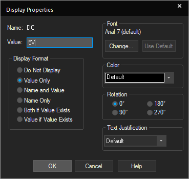
Step 19: Enter 5V for the value and click OK.
Running a Simulation
Step 20: To create a simulation profile, select PSpice > New Simulation Profile from the menu.
Step 21: The New Simulation window opens. Enter ABM_BIAS for the name and click Create.
Note: If the Simulation Manager Product Choices window opens, select the appropriate license and click OK.

Step 22: The Simulation Settings window opens. Select Bias Point for the Analysis Type to run a bias point analysis.
Step 23: Leave the default settings and click OK to create the simulation.
Step 24: Select PSpice > Run from the menu to start the simulation.
Step 25: The PSpice A/D window opens but is blank. No plots are shown during a bias point simulation. Close the window.
Step 26: To view simulation results on the schematic, select Enable Bias Voltage Display from the toolbar. The voltage at each node is shown on the schematic canvas.
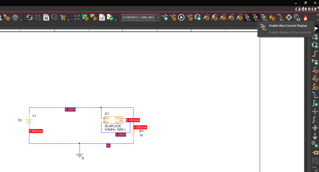
Step 27: Select Enable Bias Current Display to view the current through each mesh. With pure DC, the default Laplace model acts as a short, and the resistor draws 5V/1kΩ, 5mA.
Model Impedance in PSpice: Capacitive Impedance
Step 28: Double-click the Laplace model to open the Property Editor tab.
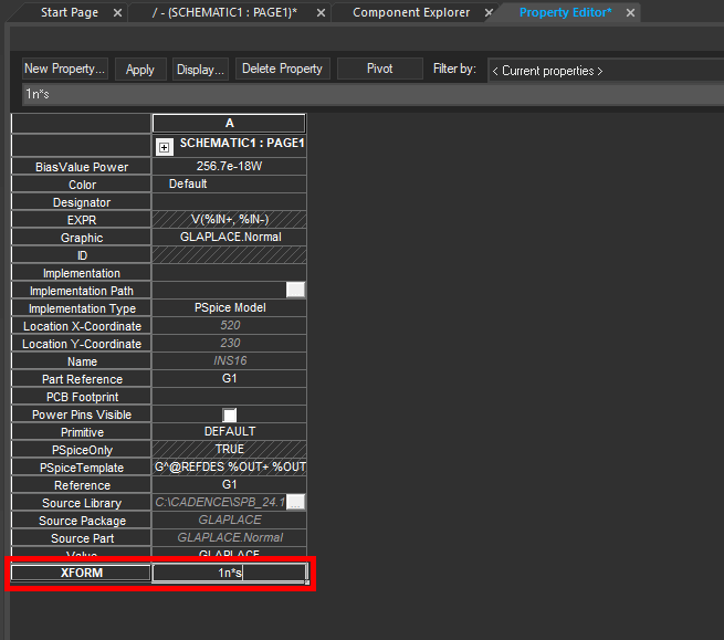
Step 29: The Property Editor tab opens, showing all properties of the Laplace model in tabular form. The XFORM row lists the Laplace expression that will be applied.
Double-click the cell and change the value to 1n*s. This will set the model susceptance to 1e-9*s, or the impedance to 1/(1e-9*s), simulating a 1nF capacitor.
Step 30: Click Apply and close the Property Editor tab.
Step 31: Select PSpice > Run from the menu.

Step 32: View the bias point results. The current through the load resistor is now close to 0A as DC is being blocked.
Close the PSpice A/D window.
Running an AC Sweep Analysis
Step 33: An AC sweep analysis can be run on this impedance ABM for better accuracy. An AC source must be present in the circuit to run an AC sweep. Select source V1 and press Delete on the keyboard.
Step 34: Select Place > PSpice Part > Source > Voltage Sources > AC from the menu. Click to place the AC source where the DC source was in the schematic, then right-click and select End Mode.
Step 35: Select PSpice > New Simulation Profile from the menu.
Step 36: Name the profile ABM_AC and click Create.
Step 37: The Simulation Settings window opens. Select AC Sweep/Noise from the Analysis Type dropdown.
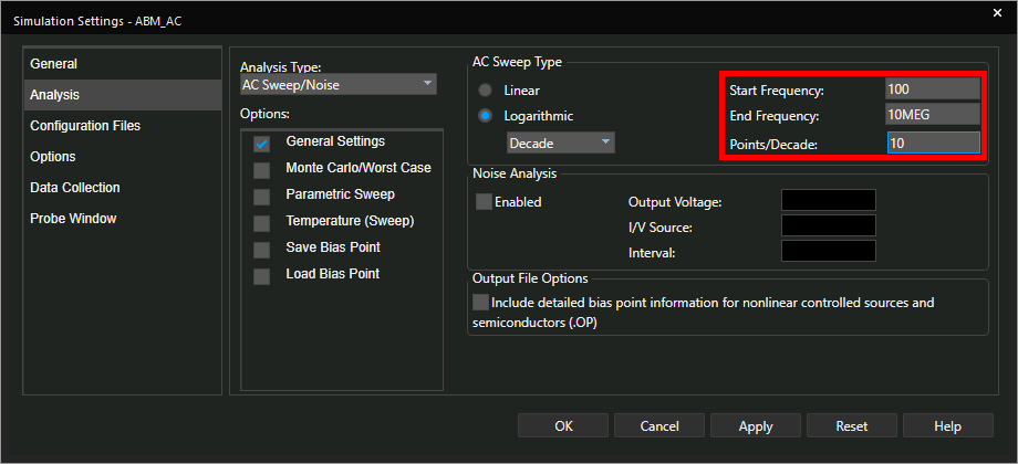
Step 38: Enter 100 for the Start Frequency, 10MEG for the End Frequency, and 10 for the Points/Decade.
Step 39: Click OK to save the settings and close the window.
Step 40: An AC sweep analysis will show the circuit output across a range of frequencies. To indicate the circuit output, a probe must be placed on the schematic canvas. Select the Voltage/Level Marker button from the toolbar.
Step 41: Click to place a probe at the output of the current source model. Right-click and select End Mode.
Step 42: Select Enable Bias Voltage Display and Enable Bias Current Display to disable bias displays.
Step 43: Select PSpice > Run from the menu.
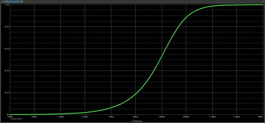
Step 44: View the simulation results. The voltage across R1 increases with frequency, as expected.
Creating a Bandpass Filter with an ABM
Step 45: More complicated impedance circuits can be simulated from their Laplace formulas as well. Close the PSpice A/D window and double-click the ABM to open the Property Editor tab.
Note: The impedance of a bandpass filter consisting of a capacitor and inductor in series can be written as:

Step 46: Double-click the XFORM value and enter 1/(47u*s+1/(100n*s)). This will simulate the admittance of a 47μH inductor and a 100nF capacitor in series.
Step 47: Click Apply and close the Property Editor tab.
Step 48: Select PSpice > Run from the menu.
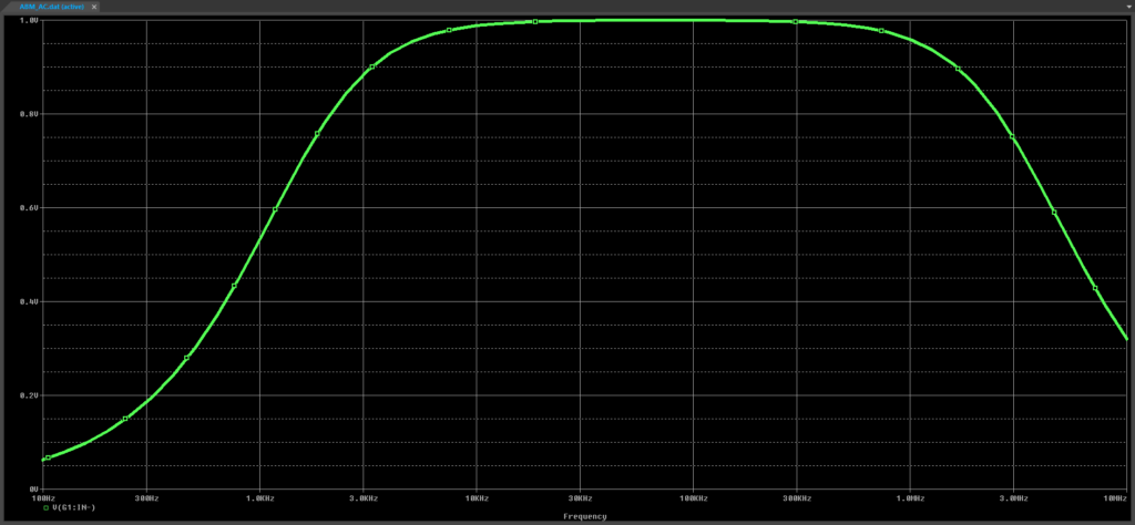
Step 49: View the simulation results. The load resistor receives full voltage between approximately 10kHz and 500kHz.
Wrap Up & Next Steps
Quickly model impedance in PSpice with analog behavioral models to ensure accurate circuit behavior. Test out this feature and more with a free trial of OrCAD. Want to learn more about PSpice? View additional how-tos, walk-throughs, and courses at EMA Academy.

