Signal integrity is critical in high-speed designs to guarantee proper circuit functionality. Electrical Rule Checks such as impedance discontinuities, unintended coupling, and reference discontinuities can create additional noise and degrade signal quality. Easily identify and resolve these common signal integrity issues during the PCB design process with electrical rule checks in Sigrity.
This how-to will provide step-by-step instructions on:
- How to use the ERC workflow in Sigrity to perform electrical rule checks
- How to analyze impedance plots, tables, and overlay results
- How to analyze coupling plots, tables and overlay results
- How to analyze references in your PCB designs
To follow along with this tutorial, use the design provided above the table of contents.
How-To Video
Electrical Rule Checks in Sigrity
Step 1: Open Sigrity Layout Workbench or any Sigrity software package and select File > Switch Workflow from the menu.
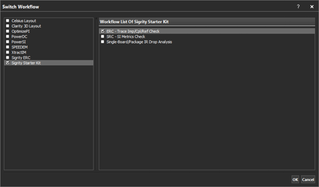
Step 2: From the tool selection list, select a software package that includes Electrical Rule Checking such as PowerSI, Sigrity ERC, or Sigrity Starter Kit. In the Workflow list, select ERC – Trace Imp/Cpl/Ref Check and click OK.
Step 3: Under Layout Setup in the workflow pane, select Load Layout File.
Step 4: Browse to the location of the provided design file, ERC_Tutorial.spd. Select the file and click Open.
Validating Board Information
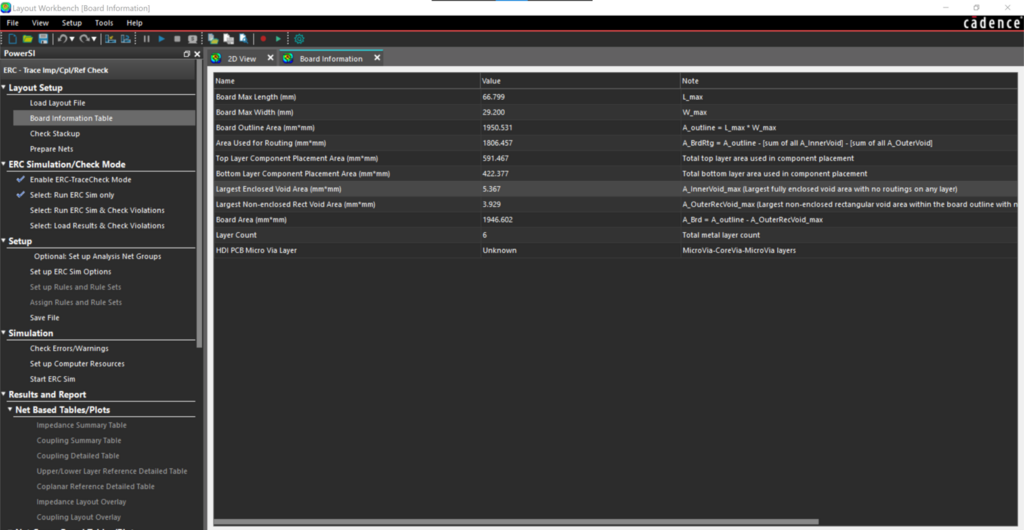
Step 5: Select Board Information Table in the workflow pane.
Note: This table displays the board information including maximum length, maximum width, board outline area, area used for routing, layer count, and more.
Step 6: Verify the board information and close the window.
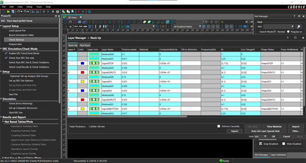
Step 7: Select Check Stackup in the workflow pane.
Note: This window allows you to view and modify the board stackup.
Step 8: Verify the board stackup and click OK to close the window.
Configuring the Simulation
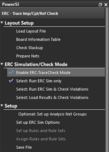
Step 9: Under ERC Simulation/Check Mode in the workflow pane, ensure Enable ERC-TraceCheck Mode and Select: Run ERC Sim Only are selected.
Note: The following modes are available for ERC trace check:
- Run ERC Sim Only: This mode is enabled by default and allows you to perform simulation on the design to analyze impedance, coupling, and references.
- Run ERC Sim & Check Violations: This mode allows you to set rules, perform simulation for impedance, coupling, and references in the design and analyze the rule violations.
- Load Results & Check Violations: This mode allows you to load results from a previous simulation, set rules, and analyze the rule violations
Based on the selection, the workflow pane automatically enables the setup requirements.
Step 10: Under Setup in the workflow pane, select Setup ERC Sim Options.
Note: Under Setup, there is an additional option to Setup Analysis Net Groups. For this design, net groups have already been configured and can be viewed in the Setup ERC Sim Options. To learn how to configure net groups for ERC Simulation, check out the Electrical Rule Checking Workshop.
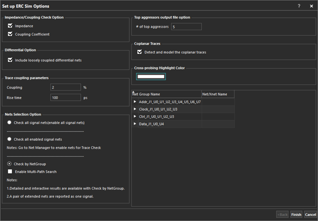
Step 11: Under Impedance/Coupling Check Option, check Impedance and Coupling Coefficient.
Step 12: Under Differential Option, select to Include loosely coupled differential nets.
Step 13: Under Trace Coupling Parameters, set the Coupling to 2% and the Rise time to 100 ps.
Step 14: Under Net Selection Option, select Check by NetGroup.
Note: With this option selected, there is an option to Enable Multi-Path Search. This option finds all the paths between any two components on the same net and reports the corresponding impedances in the generated results.
Step 15: Under Top Aggressors Output File option, set the # of Top Aggressors to 5.
Step 16: Under Coplanar Traces, select Detect and model the coplanar traces.
Step 17: Under Cross-probing Highlight Color, select the color box. Select White and click OK.
Step 18: Select Finish.
Performing Electrical Rule Checks
Step 19: Under Setup, select Save File.
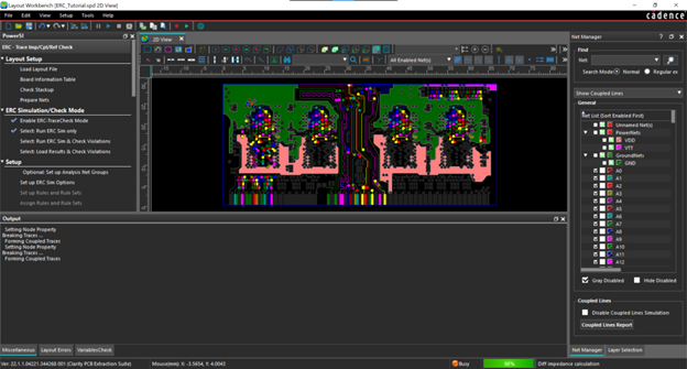
Step 20: Under Simulation, select Start ERC Sim to perform electrical rule checks.
Note: During simulation, the status is reported as busy and the progress of the simulation is shown. When the simulation is completed, the Results and Report options are automatically enabled.
Viewing Impedance Results
Step 21: Under Results and Report in the Net Group Based Tables/Plot section, select Impedance Plot (collapsed).
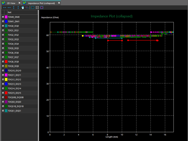
Note: The Impedance Plot (collapsed) provides detailed information about the impedance between two components: the transmitter and receiver. Components can be changed in the From/To drop-down list at the top of the Impedance Plot window.
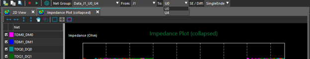
Step 22: In the To drop-down menu, select U4 as the receiver.
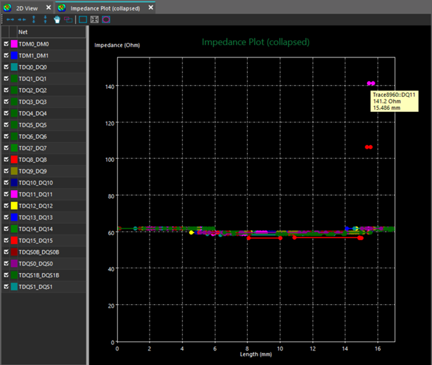
Step 23: Double-click the impedance plot at the value 141.2 Ohm.
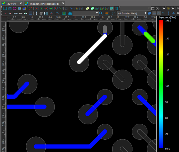
Note: The trace will be highlighted in white in in the layout window. Zoom out to see the entire trace by selecting View > Zoom > Out from the menu. Click the layout window to zoom out. Select View > Zoom > Out from the menu again to exit the mode. Select View > Zoom > Fit to see the entire PCB.
Step 24: Select the Impedance Plot (collapsed) tab. From the SE/Diff drop-down menu, select Diff.
Note: The impedance along the differential traces for the net group Data is shown from J1 to U4.
Step 25: Close the Impedance Plot (collapsed).
Step 26: Under Results and Report in the Net Group Based Tables/Plot section, select Impedance Plot (expanded).
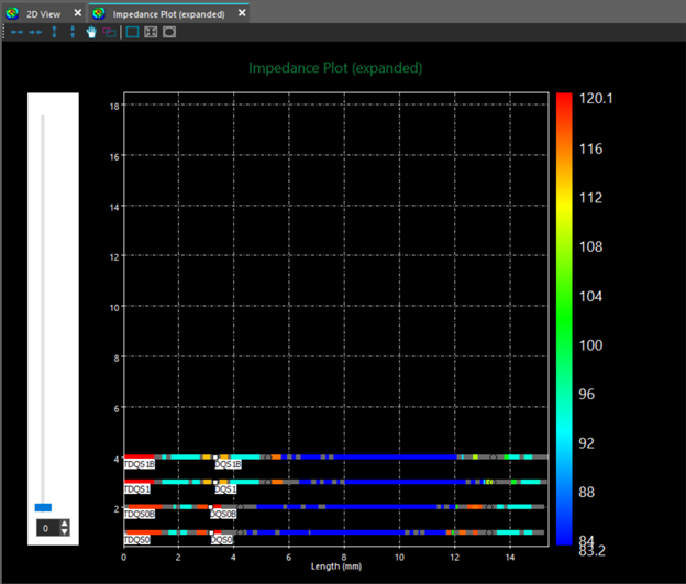
Note: The impedance of the Data net group is displayed. The colors show the different values of the impedance for each net. The following symbols are used in the expanded impedance plot:
- Square: Indicates there is a passive component on the net. Typically, the trace name will change when going through a component. Both names are displayed in the impedance plot.
- Circle: Indicates there is a via on the net.
Adjust the scroll bar on the impedance plot to obtain the desired view. Double-click a trace section in the Impedance Plot to highlight the trace using the pre-defined color in in the layout window. View either the single-ended impedance or differential impedance with selection in the SE/Diff drop-down menu.
Step 27: Close the Impedance Plot (expanded).
Step 28: Under Results and Report in the Net Group Based Tables/Plot section, select Impedance Table.
Step 29: From the SE/Diff drop-down menu, select SingleEnded.
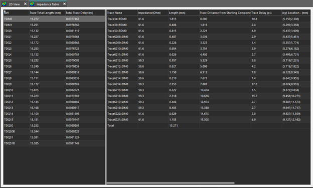
Note: The length and impedance value for each trace section on the Single-End nets are displayed in the Impedance Table. Select a net to view the related information. To view other net group information, select the desired group from the Net Group drop-down menu. To view the differential impedance, select Diff from the SE/Diff drop-down menu.
Step 30: Close the Impedance Table.
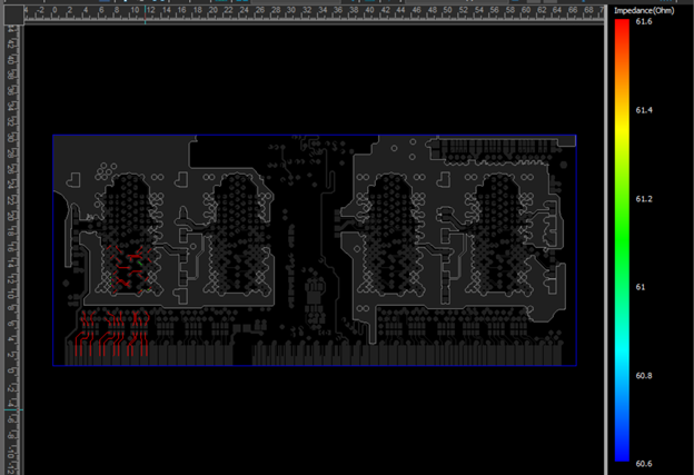
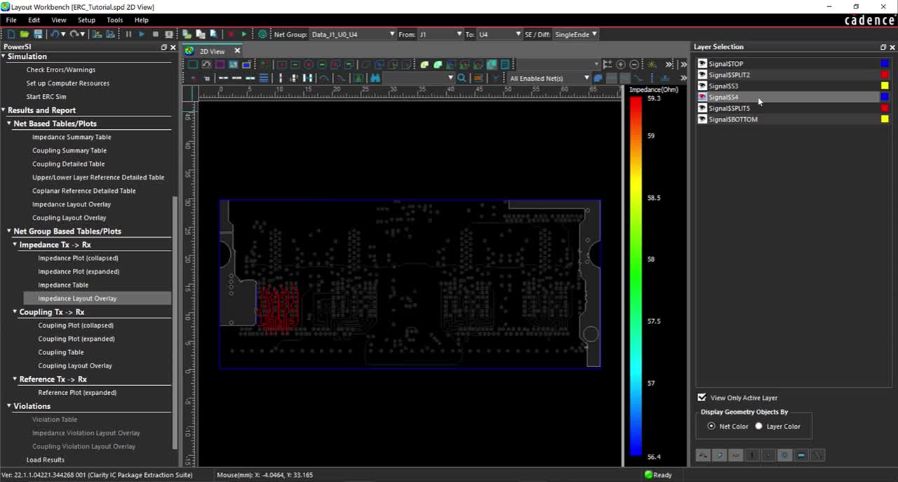
Step 31: Under Results and Report in the Net Group Based Tables/Plot section, select Impedance Layout Overlay.
Note: To view the entire board, select View > Zoom > Fit from the menu.
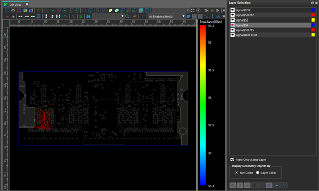
Step 32: In the Layer Selection, select Signal$S4 to view the impedance value on a different layer.
Note: If the layer selection pane is not visible, select View > Layer Selection from the menu.
Step 33: Under Results and Report in the Net Group Based Tables/Plot section, select Impedance Layout Overlay again to close the view.
Viewing Coupling Results
Step 34: In the Results and Report in the Net Group Based Tables/Plot section, select Coupling Plot (collapsed).
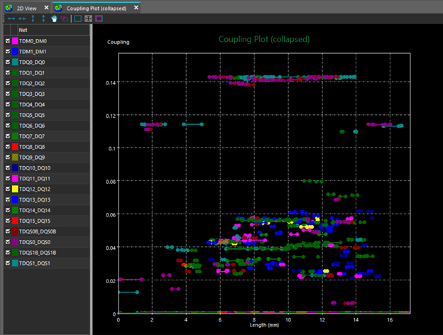
Note: The Coupling Plot (collapsed) provides detailed information about the coupling between two components, the transmitter and receiver. Components can be changed in the From/To drop-down list at the top of the Coupling Plot window.

Step 35: Right-click in the net name pane and select Disable All Nets.
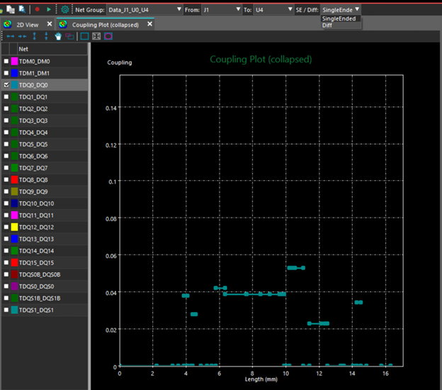
Step 36: In the Net Name pane, select TDQ0_DQ0 to enable it in the Coupling Plot.
Step 37: From the SE/Diff drop-down menu, select Diff to view the differential pair coupling.
Step 38: Close the Coupling Plot (collapsed).
Step 39: Under Results and Report in the Net Group Based Tables/Plot section, select Coupling Plot (expanded).
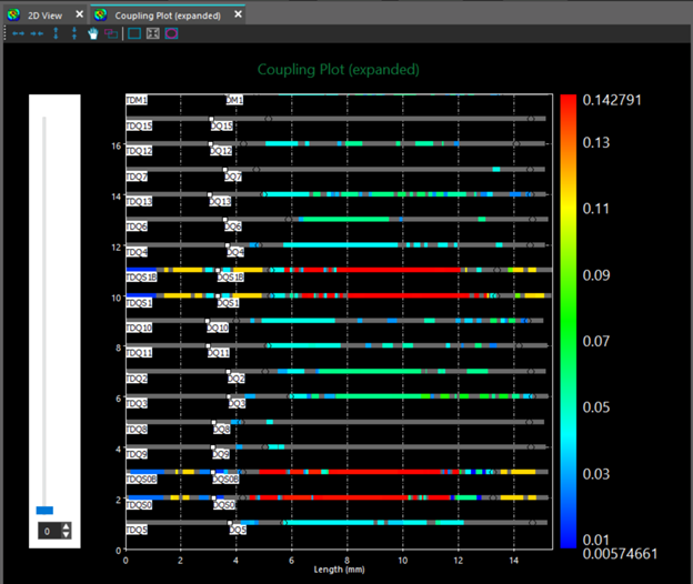
Note: The expanded coupling along the traces in the net group Data is shown. The different colors show the coupling from weakest (blue) to strongest (red). Double-click a trace selection in the coupling plot to highlight the trace using the pre-defined color in the layout window.
Step 40: Close the Coupling Plot (expanded).
Step 41: Under Results and Report in the Net Group Based Tables/Plot section, select Coupling Table.
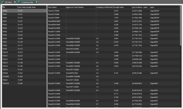
Note: The differential coupling along the traces for each section in the Net Group is displayed in the Coupling Table. Select a net to view the related information. To view other net group information, select the desired group from the Net Group drop-down menu.
Step 42: From the SE/Diff drop-down menu, select SingleEnded. Close the Coupling Table.
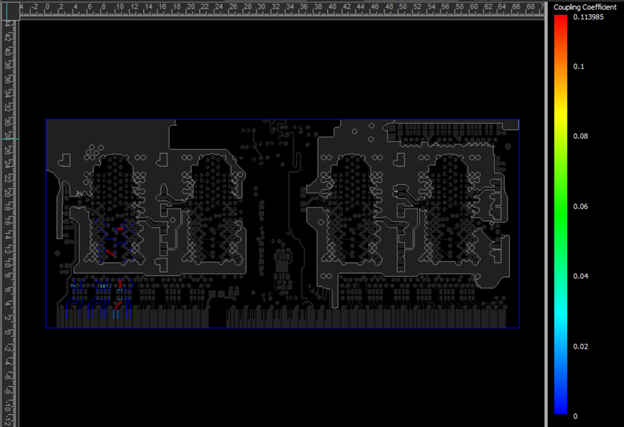
Step 43: Under Results and Report in the Net Group Based Tables/Plot section, select Coupling Layout Overlay.
Note: In the Layer Selection pane, select the desired layer to view the related coupling coefficient.
Step 44: Under Results and Report in the Net Group Based Tables/Plot section, select Coupling Layout Overlay again to close the view.
Viewing Reference Check Results
Step 45: Under Results and Report in the Net Group Based Tables/Plot section, select Reference Plot (expanded).
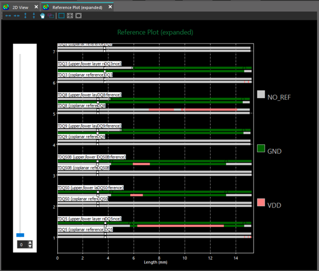
Note: The Reference plot allows you to identify reference discontinuities that can cause signal integrity issues. The names of the reference planes are displayed on the right side of the plot. The reference plot reports the following information:
- Upper/Lower Layer Reference: The reference planes directly above and below a trace segment.
- Coplanar Reference: The reference planes at two sides of a trace segment on the same layer when coplanar mode is enabled.
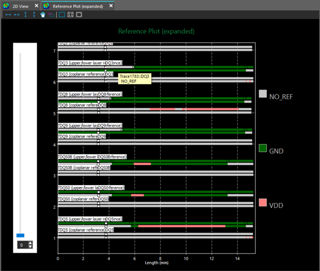
Step 46: Double-click the NO_REF portion of DQ3 for the Upper/Lower Layer Reference.
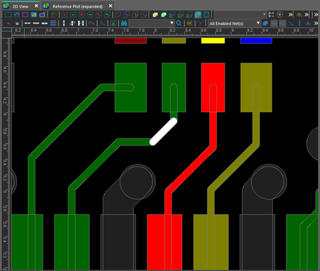
Note: The trace will be highlighted in white in in the layout window. Zoom out of the layout window to see the entire trace by selecting View > Zoom > Out from the menu. Click the Layout window to zoom out. Select View > Zoom> Out from the menu again to exit the mode. Select View > Zoom> Fit to view the entire PCB.
Step 47: Close the Reference Plot (expanded).
Wrap Up & Next Steps
Easily analyze the impedance, coupling, and references in your PCB designs to improve signal integrity with electrical rule checking in Sigrity. To learn more about this topic including configuring net groups, additional simulation results, analyzing violations, and generating reports, view our Electrical Rule Checking Workshop.

